Pixel circuit, driving method and display device of light emitting device

A technology for pixel circuits and light-emitting devices, which is applied in the fields of display devices, pixel circuits, and drivers, and can solve problems such as reduced brightness of OLED devices, life-span problems and differences in OLED devices, and achieves the effects of improving display uniformity and solving brightness unevenness

Active Publication Date: 2012-12-19
BOE TECH GRP CO LTD
View PDF7 Cites 36 Cited by
  • Summary
  • Abstract
  • Description
  • Claims
  • Application Information

AI Technical Summary

Problems solved by technology

[0004] However, OLED devices have their own life problems, that is, the electrical performance will be attenuated with the increase of use time
Therefore, during the use process, the voltage drop on the OLED device will increase, which means that the same driving voltage is used, but different driving currents are generated, resulting in a decrease in the brightness of the OLED device.
And because the performance of the OLED device on each pixel is not exactly the same, the brightness of the OLED device of each pixel changes differently, which eventually leads to uneven display brightness.

Method used


Image

  • Pixel circuit, driving method and display device of light emitting device
  • Pixel circuit, driving method and display device of light emitting device
  • Pixel circuit, driving method and display device of light emitting device

Examples


Embodiment 1

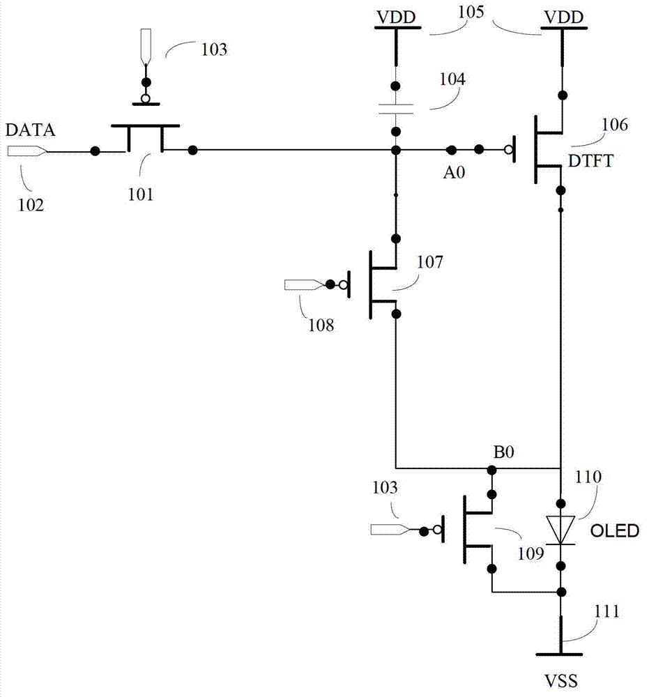
[0031] see figure 1 , a pixel circuit of a light emitting device provided in an embodiment of the present invention, comprising:

[0032] Switching transistor 101, column data line 102, row scanning line 103, first storage capacitor 104, first end of power line 105, drive transistor 106, first compensation transistor 107, OLED light emission control line 108, second compensation transistor 109, OLED 110 and the second end 111 of the power cord; and; wherein,

[0033] The source of the switching transistor 101 is connected to the column data line 102, the gate is connected to the row scanning line 103, and the drain is connected to the first terminal of the first storage capacitor 104, the first terminal of the first storage capacitor 104 The two ends are connected to the first end 105 of the power line;

[0034] The source of the drive transistor 106 is connected to the first end of the power line 105, the gate is connected to the first end of the first storage capacitor 104...

Embodiment 2

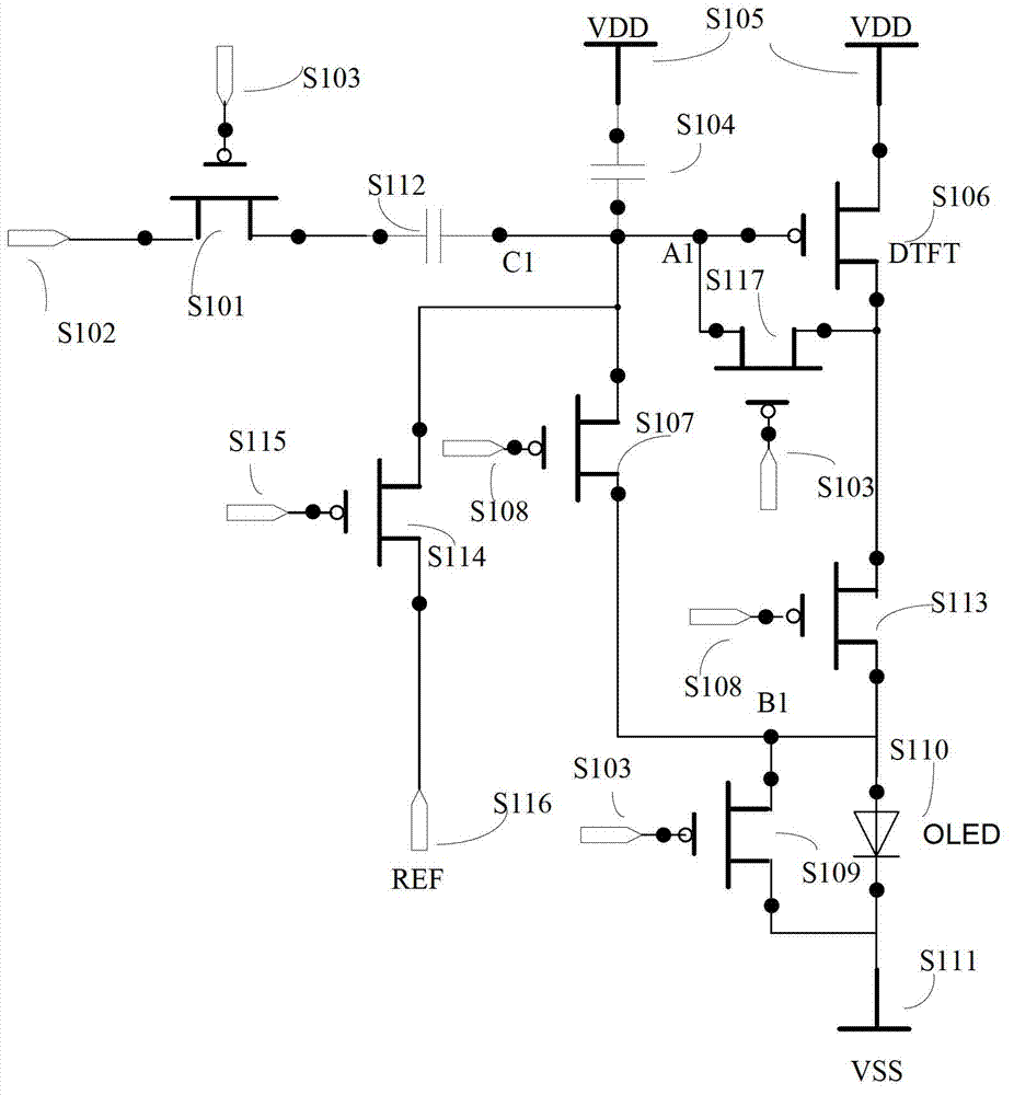
[0049] see image 3 , the pixel circuit of the light-emitting device provided in Embodiment 2 of the present invention, including:

[0050] Switching transistor S101, column data line S102, row scanning line S103, first storage capacitor S104, first end of power line S105, driving transistor S106, first compensation transistor S107, OLED light emission control line S108, second compensation transistor 109, OLED S110 and the second end S111 of the power cord; wherein,

[0051] The source of the switching transistor S101 is connected to the column data line S102, the gate is connected to the row scanning line S103, and the drain is connected to the first terminal of the first storage capacitor S104, and the first terminal of the first storage capacitor S104 The two ends are connected to the first end S105 of the power cord;

[0052] The source of the driving transistor S106 is connected to the first end of the power line S105, the gate is connected to the first end of the firs...

Embodiment 3

[0077] see Figure 5 , the pixel circuit of the active light-emitting device provided in Embodiment 3 of the present invention, including:

[0078] Switching transistor S201, column data line S202, row scanning line S203, first storage capacitor S204, first end of power line S205, drive transistor S206, first compensation transistor S207, OLED light emission control line S208, second compensation transistor S209, OLEDS 210 and the second end of the power cord S211;; wherein,

[0079]The source of the switching transistor S201 is connected to the column data line S202, the gate is connected to the row scanning line S203, the drain is connected to the first terminal of the first storage capacitor S204, and the first terminal of the first storage capacitor S104 The two ends are connected to the first end S205 of the power cord;

[0080] The source of the driving transistor S206 is connected to the first end of the power line S205, the gate is connected to the first end of the f...


PUM


Abstract

The invention discloses a pixel circuit, a driving method and a display device of a light emitting device, avoiding the attenuation of an OLED (organic light emitting diode). In the circuit, a source of a switch transistor is connected with a line data wire; a grid is connected with a row scanning line; a drain is connected with a first end of a first storage capacitor; a second end of the first storage capacitor is connected with a first end of a power supply wire; a source of a driving transistor is connected with the first end of the power supply wire; the grid is connected wit the first end of the first storage capacitor; the drain is connected with the first end of the OLED; a source of a first compensating transistor is connected with the first end of the first storage capacitor; a grid of the first compensating transistor is connected with a light emitting control wire; a drain of the first compensating transistor is connected with a source of the second compensating transistor and the first end of the OLED; a grid of the second compensating transistor is connected with the row scanning line; and a drain of the second compensating transistor is connected with second end of the OLED and the second end of the power supply wire. The display device comprises a pixel circuit of the light emitting device.

Description

technical field [0001] The invention relates to the field of display technology, in particular to a pixel circuit of a light emitting device, a driving method and a display device. Background technique [0002] The light-emitting element of an active light-emitting diode display (AMOLED) is an organic light-emitting diode (OLED), and its luminous brightness is proportional to the magnitude of the driving current supplied to the OLED device. Therefore, in order to achieve the best display effect, a large driving current is required . The low-temperature polysilicon backplane technology is the best choice for AMOLED display backplane technology because it can provide higher mobility. [0003] The problem of threshold voltage drift inherent in low-temperature polysilicon technology will cause non-uniformity of the driving current generated by the pixel circuit, and thus non-uniformity of display brightness. In order to effectively compensate for the drift of the threshold vol...

Claims


Application Information

Patent Timeline
Patent Type & Authority Applications(China)
IPC IPC(8): H01L27/32G09G3/32G09G3/3233
Inventor 王颖
Owner BOE TECH GRP CO LTD
Why Eureka
Try Eureka