
bias circuit

A bias circuit, bias current technology, applied in electrical components, amplifiers with semiconductor devices/discharge tubes, improving amplifiers to reduce temperature/power supply voltage changes, etc., to achieve the effect of suppressing temperature dependence

Active Publication Date: 2016-03-16
SEMICON COMPONENTS IND LLC
View PDF2 Cites 0 Cited by
  • Summary
  • Abstract
  • Description
  • Claims
  • Application Information

AI Technical Summary

Problems solved by technology

[0004] However, in bipolar transistors, parameters such as the base-emitter voltage VBE and the DC current amplification factor hfe are temperature-dependent

Method used


Image

  • bias circuit
  • bias circuit
  • bias circuit

Examples


Embodiment Construction

[0019] Hereinafter, embodiments of the present invention will be described based on the drawings.

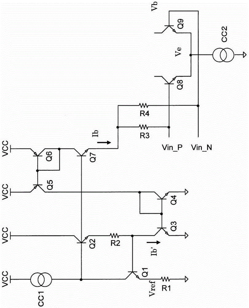
[0020] figure 1 The circuit configuration including the bias circuit according to the embodiment is shown.

[0021] The emitters of the NPN differential transistors Q8 and Q9 are connected in common, and the emitters are connected to the ground via the constant current circuit CC2. Here, the emitter voltages of the differential transistors Q8 and Q9 are set to Ve. The differential transistors Q8 and Q9 are part of the differential amplifier, and provide a pair of complementary signals, namely the signal Vin_P and the signal Vin_N to the bases of the differential transistors Q8 and Q9. Furthermore, bias currents are supplied to the bases of the transistors Q8 and Q9 via resistors R3 and R4, respectively.

[0022] The current value Ib, which is the sum of the currents flowing through the resistors R3 and R4, is the base current (bias current) of the differential transistors Q8 and Q9 ...


PUM


Abstract

The bias circuit of the present invention is used to suppress the temperature dependence of the emitter voltage of the operating transistor. The bias current Ib is supplied to the base of the action transistor Q8 via the first resistors R3, R4 and the first transistor Q7. Comprising at least one current mirror circuit, a corresponding current Ib' corresponding to the bias current Ib flows through the second transistor Q3. The third transistor Q2 is connected to the base of the first transistor in common, and a corresponding current Ib' flows through, and the second resistor R2 obtains a voltage drop corresponding to the voltage drop in the above-mentioned first resistor R3. The fourth transistor Q1 receives the reference voltage Vref on the emitter side, and the base is connected to the emitter side of the above-mentioned third transistor Q2. 1VBE of the operating transistor Q8 is canceled by 1VBE of the fourth transistor Q1, and 1VBE of the second transistor Q7 is canceled by 1VBE of the third transistor Q2, thereby setting the reference voltage Vref on the emitter side of the operating transistor Q8.

Description

Technical field [0001] The present invention relates to a bias circuit that supplies a bias current to the base of an action transistor. Background technique [0002] In the past, in differential amplifiers, etc., such as Figure 4 A pair of differential transistors Q51 and Q52 in which the emitters are connected in common as shown, and the emitters are connected to a constant current circuit. Furthermore, the signal is input to the differential transistors Q51 and Q52, but the differential transistor is supplied with a bias current from the bias circuit and can perform an operation corresponding to the input signal. [0003] in Figure 4 There are power supply V51, resistors R51, R52, and the output voltage of the power supply V51 is supplied to the bases of differential transistors Q51, Q52 via resistors R51, R52 as bias voltages. [0004] However, in a bipolar transistor, parameters such as the base-emitter voltage VBE and the DC current amplification factor hfe have temperature de...

Claims


Application Information

Patent Timeline
Patent Type & Authority Patents(China)
IPC IPC(8): H03F1/30H03F3/45
CPCH03F3/45085H03F2200/447H03F2203/45622
Inventor 盐田智基
Owner SEMICON COMPONENTS IND LLC
Learn More