A key detection circuit and detection method

A detection circuit and detection method technology, which is applied in the key field, can solve the problems of complex circuit design, poor practicability, and high production cost, and achieve the effects of reducing production cost, strong applicability, and high reliability

Active Publication Date: 2016-03-09
HISENSE BROADBAND MULTIMEDIA TECH
View PDF3 Cites 0 Cited by
  • Summary
  • Abstract
  • Description
  • Claims
  • Application Information

AI Technical Summary

Problems solved by technology

For example, when the number of GPIOs is 3, the number of buttons is also 3, so it is necessary to add identifiable buttons without changing the number of GPIOs, which can only be realized by adding additional devices, which makes the circuit design more complicated. At the same time, the production cost is also high and the practicability is low
The existing matrix scanning circuit used in the market can realize the real-time detection of 9 buttons through 6 GPIOs, but this still requires a large number of GPIOs to realize the real-time scanning of the buttons, the practicability is still not strong, and the production cost is high

Method used


Image

  • A key detection circuit and detection method
  • A key detection circuit and detection method

Examples


Embodiment 1

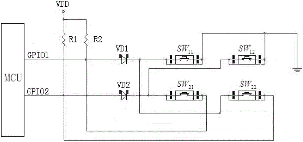
[0046] figure 1 It shows a circuit diagram in which the CPU sets two GPIO interfaces to detect 4 keys. Such as figure 1 as shown,

[0047] The button detection circuit includes the central processing unit MCU, 4 buttons SW 11 、SW 12 、SW 21 、SW 22 and power supply, the central processing unit MCU is set with GPIO 1 , GPIO 2 Two GPIO interfaces, GPIO 1 , GPIO 2 respectively through pull-up resistors R 1 , R 2 Connect to power supply. Among them GPIO 1 , GPIO 2 Constitute 4 detection circuits.

[0048] When GPIO 1 , GPIO 2 When both are input interfaces: GPIO 1 , GPIO 2 Respectively via the button SW 11 、SW 12 Grounded to form 2 detection lines;

[0049] When GPIO 1 For the output interface, GPIO 2 When it is an input interface: GPIO 2 by SW 21 with GPIO 1 Composition detection SW 21 detection line;

[0050] When GPIO 2 For the output interface, GPIO 1 When it is an input interface: GPIO 1 by SW 22 with GPIO 2 Composition detection SW 22 detectio...

Embodiment 2

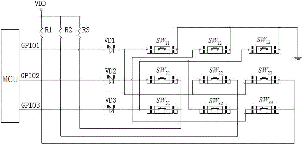
[0059] figure 2 It shows a circuit diagram in which the central processing unit sets three GPIO interfaces to realize detection of 9 keys. Such as figure 2 As shown, the button detection circuit includes a central processing unit MCU, 9 buttons and a power supply, and the central processing unit MCU is provided with GPIO 1 , GPIO 2 , GPIO 3 Three GPIO interfaces, GPIO 1 , GPIO 2 , GPIO 3 respectively through pull-up resistors R 1 , R 2 , R 3 Connect to power supply. Among them GPIO 1 , GPIO 2 , GPIO 3 Three GPIO interfaces form nine detection circuits.

[0060] When all three GPIOs are input interfaces: GPIO 1 , GPIO 2 , GPIO 3 Respectively via the button SW 11 、SW 12 、SW 13 Grounded to form 3 detection lines;

[0061] When GPIO 1 For the output interface, GPIO 2 , GPIO 3 When it is an input interface: GPIO 2 by SW 21 with GPIO 1 Composition detection SW 21 detection line; GPIO 3 by SW 31 with GPIO 1 Composition detection SW 31 detection line; ...


PUM


Abstract

The invention discloses a key detection circuit comprising a central processing unit MCU (microprogrammed control unit), n2 keys and a power source. The central processing unit MCU is provided with n general purpose input / output (GPIO) interfaces. The n2 keys are arranged according to a SW<nxn> matrix. A key detection circuit comprises n2 detection lines: when all GPIO interfaces are input interfaces, the GPIO is earthed via the key SW1m to form a SW<1m> detection line; when the GPIO is an output interface while the GPIO<1> to GPIO<i-1> and the GPIO<i+1> to the GPIO <n> are respectively connected with the GPIO to form n-1 detection lines via SW<2i>, SW<3i>, SW<4i>...and SW<ni>, and the detection lines are used for detecting the SW<2i>, the SW<3i>, the SW<4i>...and the SW<ni>. The key detection circuti can realize real-time scanning of a great quantity of keys without many GPIOs, system resources can be greatly saved, production cost is reduced, and the key detection circuit has the advantages of high reliability and applicability.

Description

technical field [0001] The invention relates to key technology, in particular to a key detection circuit. Background technique [0002] When a system has fewer general-purpose input / output interfaces (GPIO for short), it usually can only support fewer buttons, and the number of GPIOs is the same as the number of detection buttons. For example, when the number of GPIOs is 3, the number of buttons is also 3, so it is necessary to add identifiable buttons without changing the number of GPIOs, which can only be realized by adding additional devices, which makes the circuit design more complicated. Simultaneously production cost is also high, and practicality is lower. The existing matrix scanning circuit used in the market can realize the real-time detection of 9 buttons through 6 GPIOs, but this still requires a large number of GPIOs to realize the real-time scanning of the buttons, the practicability is still not strong, and the production cost is high. [0003] Therefore, i...

Claims


Application Information

Patent Timeline
Patent Type & Authority Patents(China)
IPC IPC(8): H03M11/20
Inventor 刘永波
Owner HISENSE BROADBAND MULTIMEDIA TECH
Why Eureka
Try Eureka