Backside illumination sensor having a bonding pad structure and method of making the same

A bonding pad and radiation sensor technology, applied in semiconductor/solid-state device manufacturing, electrical solid-state devices, semiconductor devices, etc., can solve problems such as bonding pad peeling or other defects

Active Publication Date: 2013-01-09
TAIWAN SEMICON MFG CO LTD
View PDF6 Cites 34 Cited by
  • Summary
  • Abstract
  • Description
  • Claims
  • Application Information

AI Technical Summary

Problems solved by technology

The problem with thin metal layers is that bond pads formed in such layers can exhibit peeling or other defects

Method used


Image

  • Backside illumination sensor having a bonding pad structure and method of making the same
  • Backside illumination sensor having a bonding pad structure and method of making the same
  • Backside illumination sensor having a bonding pad structure and method of making the same

Examples


Embodiment Construction

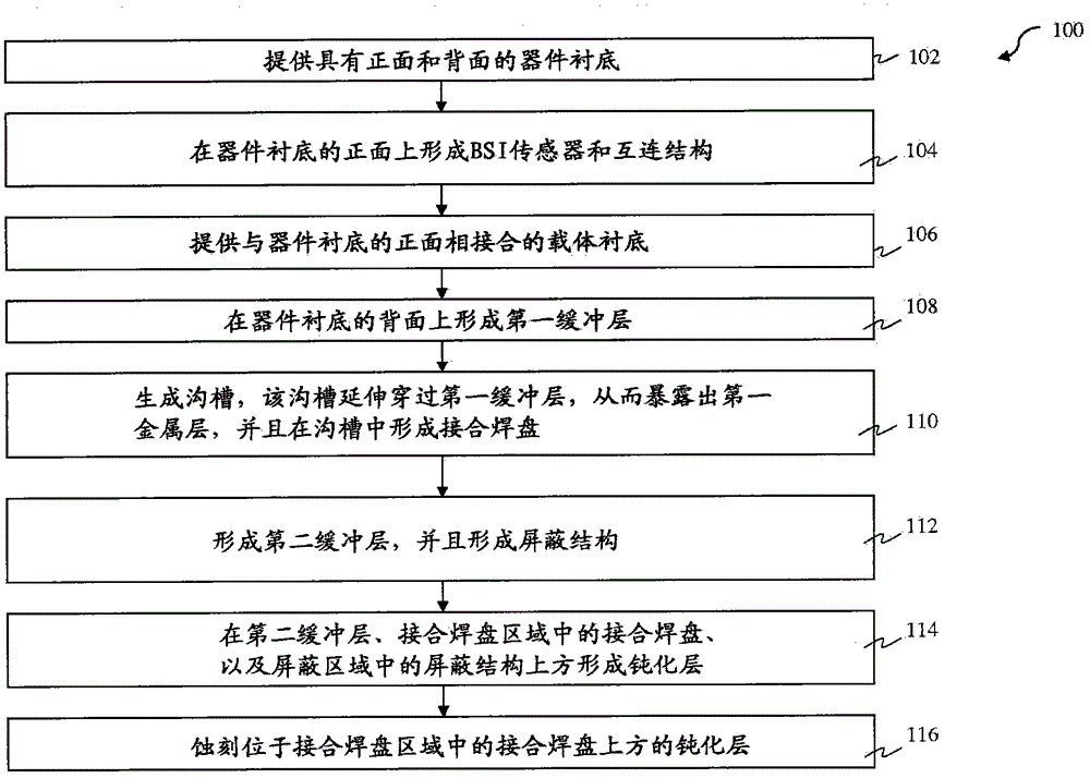
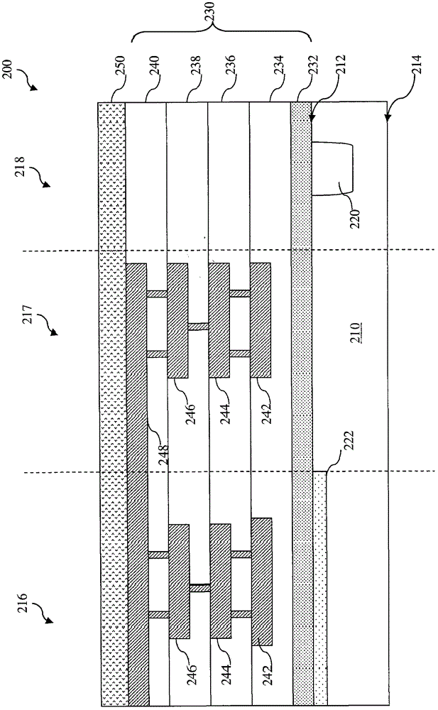
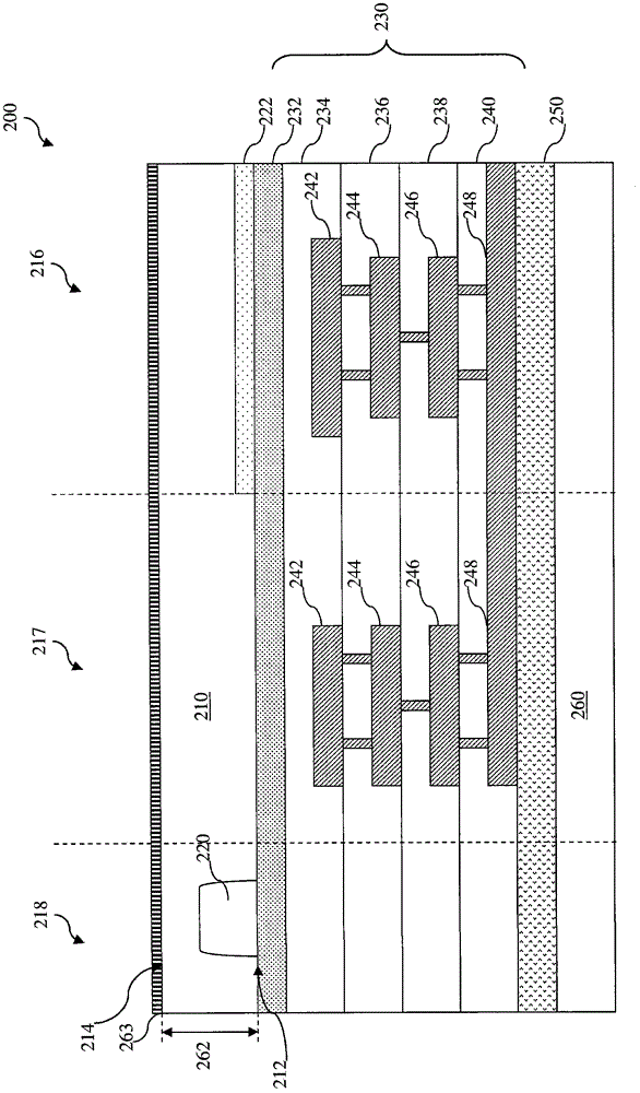
[0031] The following disclosure provides a number of different embodiments or examples for implementing different features of the present invention. Specific examples of components and arrangements are described below to simplify the present disclosure. Of course, these are only examples and are not intended to limit the invention. For example, in the following description, forming a first component over or on a second component may include embodiments in which the first component and the second component are in direct contact, and may also include that other components may be formed between the first component and the second component An embodiment such that the first part and the second part are not in direct contact. In addition, the present invention may repeat reference numerals and / or symbols in multiple instances. This repetition is for simplicity and clarity, and does not in itself indicate a relationship between the various embodiments and / or configurations describe...


PUM


Abstract

The present disclosure provides one embodiment of a semiconductor structure. The semiconductor structure comprises a device substrate having a front side and a back side; an interconnect structure disposed on the front side of the device substrate; and a bonding pad connected to the interconnect structure. The bonding pad comprises a recessed region in a dielectric material layer; a dielectric mesa of the dielectric material layer interposed between the recessed region; and a metal layer disposed in the recessed region and on the dielectric mesa.

Description

[0001] Cross References to Related Applications [0002] This application is related to the following commonly assigned U.S. patent application, the entire disclosure of which is incorporated herein by reference: U.S. Patent Application Serial No. 13 / 112,828 (Attorney Docket: 2011-0239 / 24061.1814), entitled "Semiconductor Device Having a Bonding Pad and Shield Structure and Method of Manufacturing the Same," and U.S. Patent Application No. 13 / 112,755 (Attorney Docket No. 2011-0379 / 24061.1815), entitled "Semiconductor Device Having a Bonding Pad and Method of Manufacturing the Same Same". technical field [0003] The present invention relates to the field of semiconductors, and more particularly, the present invention relates to a back-illuminated sensor with a bonding pad structure and a manufacturing method thereof. Background technique [0004] The semiconductor integrated circuit (IC) industry has undergone rapid development. Technological advances in IC materials and d...

Claims


Application Information

Patent Timeline
Patent Type & Authority Applications(China)
IPC IPC(8): H01L27/146
CPCH01L27/1464H01L2224/05096H01L27/146H01L27/14636H01L2224/05567H01L2224/48624H01L2224/05647H01L2224/05568H01L2924/01322H01L2224/04042H01L2224/05548H01L31/113H01L24/05H01L23/485H01L2224/45144H01L2224/05022H01L2224/131H01L2224/05572H01L2224/0362H01L2224/0345H01L2224/0401H01L27/14623H01L2224/05624H01L2224/05555H01L2224/48647H01L2924/3025H01L2924/15788H01L2924/12042H01L2924/12043H01L21/76898H01L23/481H01L2924/00014H01L2924/00012H01L2924/014H01L2924/00
Inventor 蔡双吉杨敦年林政贤刘人诚王文德林月秋
Owner TAIWAN SEMICON MFG CO LTD
Why Eureka
Try Eureka