Semiconductor packaging device with magnetic shielding function and production method thereof

A technology for packaging devices and semiconductors, which is applied in the manufacture of semiconductor/solid-state devices, semiconductor devices, and components of semiconductor/solid-state devices, etc., can solve the problems of poor magnetic shielding effect, etc., and achieve the effect of obvious magnetic shielding effect.

Active Publication Date: 2013-02-06
KUSN ZHONGDI MATERIALS TECH
View PDF3 Cites 7 Cited by
  • Summary
  • Abstract
  • Description
  • Claims
  • Application Information

AI Technical Summary

Problems solved by technology

[0004] In view of the above deficiencies in the prior art, the purpose of the present invention is to provide a semiconductor packaging device with magn...

Method used


Image

  • Semiconductor packaging device with magnetic shielding function and production method thereof
  • Semiconductor packaging device with magnetic shielding function and production method thereof
  • Semiconductor packaging device with magnetic shielding function and production method thereof

Examples


Embodiment Construction

[0025] The present invention provides a semiconductor packaging device with magnetic shielding function and its manufacturing method. In order to make the purpose, technical solution and effect of the present invention clearer and clearer, the present invention will be further described in detail below. It should be understood that the specific embodiments described here are only used to explain the present invention, not to limit the present invention.

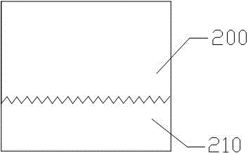
[0026] Such as figure 1 as shown, figure 1 The semiconductor package device with magnetic shielding function provided by the present invention includes a semiconductor package device body 200 and a magnetically permeable material 210 attached to the surface of the semiconductor package device body 200, and the magnetically permeable material 210 is It is pasted on the surface of the semiconductor package device body 200 by glue bonding, molding, spraying or printing. The semiconductor packaging device in the present inventi...


PUM

PropertyMeasurementUnit
Current densityaaaaaaaaaa

Abstract

The invention discloses a semiconductor packaging device with a magnetic shielding function and a production method thereof. The semiconductor packaging device comprises a semiconductor packaging device main body and a magnetic conduction material which is attached on the surface of the semiconductor packaging device, and the magnetic conduction material is attached on the surface of the semiconductor packaging device through adhesive, die-casting forming, coating or printing. The shielding effect of the semiconductor packing device such as a storage card within the high-frequency range (more than 300MHz) is similar to that of aluminum foil, the shielding effect of the semiconductor packaging device in the medium-low frequency range (less than 300MHz) is similar to no interference effect, and the shielding effect is obvious.

Description

technical field [0001] The invention relates to the field of electronic devices with a shielding function, in particular to a semiconductor packaging device with a magnetic shielding function and a manufacturing method thereof. Background technique [0002] Semiconductor packaging devices, specifically memory cards, have been used in various electronic devices. These devices often interfere with other nearby sensitive components and generate electromagnetic interference when they are working. Therefore, the market for semiconductor packaging devices with magnetic shielding function The demand is great. [0003] The American Sandisk Company applied for a patent application in 2011, which disclosed two shielding solutions, one of which is to use a metal conductive layer to directly adhere the metal conductive layer to one side of the memory card through the PMC epoxy packaging process to achieve shielding and a fixed solution; the other is to use the inkjet printing technolog...

Claims


Application Information

Patent Timeline
IPC IPC(8): H01L23/552H01L21/56
Inventor 刘伟德
Owner KUSN ZHONGDI MATERIALS TECH
Why Eureka
Try Eureka