Device for correcting offset correction between pixels of image sensor and correction method thereof

An image sensor, offset correction technology, applied in image analysis, image communication, image data processing and other directions, can solve problems such as correction errors, lattice noise, etc., to reduce parts, reduce parts and assembly costs, and simplify PCB wiring Effect

Inactive Publication Date: 2013-03-06
HYUNDAI MOBIS CO LTD
View PDF9 Cites 6 Cited by
  • Summary
  • Abstract
  • Description
  • Claims
  • Application Information

AI Technical Summary

Problems solved by technology

[0023] Therefore, the object of the present invention is to provide a pixel-to-pixel offset correction device of an image sensor, which can solve the problem of offset correction when there are dead pixels in the same pixel group when correcting the offset between Gr pixels and Gb pixels. Correction errors during the process lead to problems such as lattice noise
[0024] Another object of the present invention is to provide a method for inter-pixel offset correction of an image sensor, which can solve problems such as grid noise caused by correction errors during the offset correction process

Method used


Image

  • Device for correcting offset correction between pixels of image sensor and correction method thereof
  • Device for correcting offset correction between pixels of image sensor and correction method thereof
  • Device for correcting offset correction between pixels of image sensor and correction method thereof

Examples


Embodiment Construction

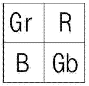
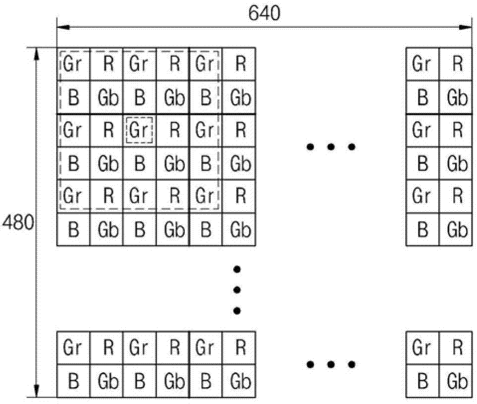
[0043] In one embodiment of the present invention, it is disclosed that when there are dead pixels in the same type of pixel group in the 5x5 window based on the mathematical formula calculation for Gr and Gb inter-pixel offset correction, by and except the dead pixels This is an inter-pixel offset correction method for an image sensor where offset correction occurs by calculating the same type of normal pixels.

[0044] In addition, an embodiment of the present invention discloses that the technical composition of identifying the edge (Edge) area is added to the inter-pixel offset correction method according to an embodiment of the present invention, and the edge area is bypassed during offset correction. A method of deskew that maintains sharpness in parts with contrast between light and dark.

[0045] An embodiment of the present invention will be described in detail below with reference to the accompanying drawings.

[0046] Figure 6 is a block diagram showing an inter-...


PUM


Abstract

The present invention uses the normal same pixel besides the dead pixel to calculate so as to prevent the error which may occured in offset correction when dead pixel exists in the same pixel group in the window with specific size for correcting the offset between Gr pixel and Gb pixel. Besides, an Edge area identification function is added so that bypass occures during the offset correction in the Edge area so as to maintain the boldness of the light and shade contrast part.

Description

[0001] technology area [0002] The present invention relates to an image sensor inter-pixel offset correction device and correction method thereof, in particular to an inter-pixel offset correction device for correcting the offset (offset or cross-talk) between a Gr pixel and a Gb pixel in a pixel and its Calibration method. Background technique [0003] In a CMOS image sensor (CMOS Image Sensor, hereinafter referred to as CIS), the image signal processing (Image Signal Processing, hereinafter referred to as ISP) block is used as a block that corrects or processes the input image through a prescribed mathematical calculation method. Its main function This is to correct the inevitable degradation of image quality due to the physical structure of pixels. [0004] figure 1 It is a drawing showing the general RGB color filter structure. [0005] refer to figure 1 , the ISP block is basically required to have, in use figure 1 The general RGB color filter shown is a function t...

Claims


Application Information

Patent Timeline
Patent Type & Authority Applications(China)
IPC IPC(8): H04N5/367
CPCH04N9/646G06T7/13
Inventor 金建杓
Owner HYUNDAI MOBIS CO LTD
Why Eureka
Try Eureka