Method for manufacturing array substrate

A manufacturing method and array substrate technology, applied in semiconductor/solid-state device manufacturing, optics, instruments, etc., can solve problems such as not detailed one by one, and achieve the effect of avoiding parasitic capacitance and improving Flicker

Active Publication Date: 2015-03-25
BOE TECH GRP CO LTD
View PDF4 Cites 0 Cited by
  • Summary
  • Abstract
  • Description
  • Claims
  • Application Information

AI Technical Summary

Problems solved by technology

[0013] It should be understood that although the existing technical defects are explained by taking the ADS liquid crystal panel as an example, similar problems also exist in the manufacture of other types of array substrates, and will not be described in detail here.

Method used


Image

  • Method for manufacturing array substrate
  • Method for manufacturing array substrate
  • Method for manufacturing array substrate

Examples


Embodiment Construction

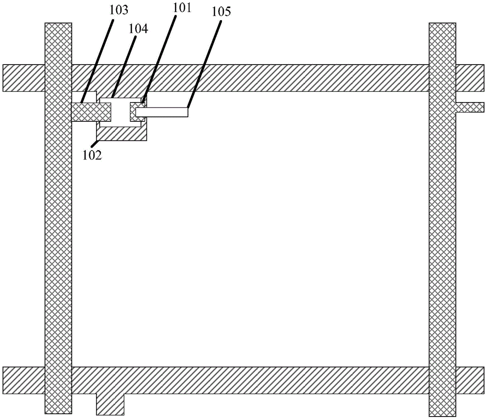
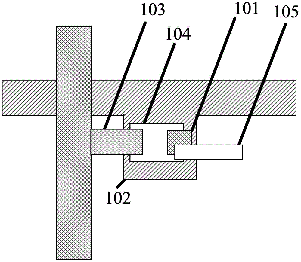
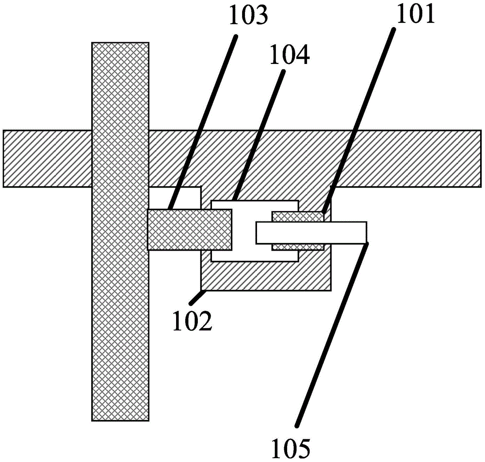
[0043]In the manufacturing method of the array substrate, the array substrate and the display device according to the embodiment of the present invention, after forming the semiconductor layer and the source-drain electrode layer for making the source-drain electrodes, the source-drain electrodes are not directly made, but reserved for Form the semiconductor layer and the source-drain electrode layer in the region of the source-drain electrode layer, and then after forming a transparent conductive layer (such as a commonly used ITO layer), process the transparent conductive layer to form an extension extending to the position where the source electrode is scheduled to be formed, Finally, the source-drain electrode layer located outside the predetermined position for forming the source-drain electrode in the reserved area is removed to finally form the source-drain electrode. In the above manner, the overlapping part of the extension part and the gate electrode is completely loc...


PUM


Abstract

The invention provides a method for manufacturing an array substrate, the array substrate and a display device. The method for manufacturing the array substrate comprises the steps that through the picture composition technology, a pattern of a semiconductor layer located in a first zone and a pattern of a source and drain electrode layer located in the first zone are formed, wherein the first zone is a preset zone used for enabling a source electrode and a drain electrode of a thin film transistor to be formed; a transparent conductive layer is formed on the portion, with the source and drain electrode layer of the first zone reserved, of a substrate; through the picture composition technology, a pattern of a first transparent electrode and a pattern of an extending portion are formed; the extending portion extends to the portion above a first position where the source electrode is formed in a preset mode, wherein the first position is in the first zone; through the picture composition technology, the portions, outside the first position and a second position, of the source and drain electrode layer are removed, so that a pattern of the source electrode and a pattern of the drain electrode are formed, wherein the second position is a position where the drain electrode is formed in a preset mode. According to the method for manufacturing the array substrate, image quality is improved.

Description

technical field [0001] The invention relates to the field of display technology, in particular to a method for manufacturing an array substrate. Background technique [0002] TFT-LCD (Thin-Film Transistor Liquid Crystal Display, Thin-Film Transistor Liquid Crystal Display) includes a color filter substrate, an array substrate and a liquid crystal layer located between the color filter substrate and the array substrate, the array substrate includes a transparent substrate, and a A plurality of gate lines parallel to each other on the transparent substrate and a plurality of data lines intersecting with the gate lines and electrically insulated, wherein two adjacent gate lines and two adjacent data lines enclose a pixel unit. [0003] Each pixel unit includes a pixel electrode, a storage capacitor C s , LCD capacitance C lc and a TFT (Thin Film Transistor) as a switching device, C s and C lc connected to the pixel electrode in parallel, and the pixel electrode is connected...

Claims


Application Information

Patent Timeline
Patent Type & Authority Patents(China)
IPC IPC(8): H01L21/28H01L21/336H01L27/12H01L29/417H01L29/786G02F1/1362G02F1/1368H01L21/84
CPCH01L27/1214H01L27/1259
Inventor 严允晟金熙哲
Owner BOE TECH GRP CO LTD
Why Eureka
Try Eureka