nor flash memory, method for forming the same, and method for forming a contact hole

A memory and contact hole technology, which is used in the manufacture of electrical solid-state devices, semiconductor devices, and semiconductor/solid-state devices, etc., can solve the problems of leakage current, insignificant leakage current of NOR flash memory, and dielectric layer breakdown, etc. The effect of expanding the minimum distance, reducing leakage current and small line width

Active Publication Date: 2015-08-05
SEMICON MFG INT (SHANGHAI) CORP
View PDF3 Cites 0 Cited by
  • Summary
  • Abstract
  • Description
  • Claims
  • Application Information

AI Technical Summary

Problems solved by technology

[0003] In addition, due to the continuous shrinking of the critical dimensions of integrated circuits, the minimum distance between the contact hole on the drain and the gate is getting smaller and smaller, causing the dielectric layer between them to be more easily broken down under high voltage, resulting in leakage current
When the device size is relatively large, the leakage current caused by the above reasons is not obvious to NOR flash memory

Method used


Image

  • nor flash memory, method for forming the same, and method for forming a contact hole
  • nor flash memory, method for forming the same, and method for forming a contact hole
  • nor flash memory, method for forming the same, and method for forming a contact hole

Examples


Embodiment Construction

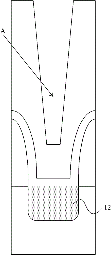
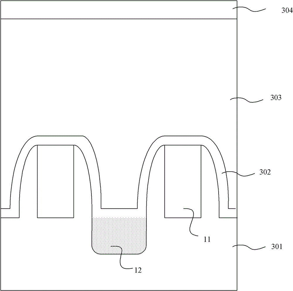
[0059]As mentioned in the background art, when the NOR flash memory operates at high voltage for erasing and writing, electrons from the source are accelerated to the drain, and then electrons are injected from the drain to the floating gate. In such a process, leakage current is easily generated between the drain and the gate due to high voltage.

[0060] After research, it is found that the leakage current is mainly concentrated between the data line (Bit-line) connected to the drain and the control line (Word-line) connected to the gate. The inventor believes that due to the continuous reduction of the critical dimensions of integrated circuits, the minimum distance between the contact hole on the drain electrode and the gate, especially between the data line (Bit-line) and the control line (Word-line) is getting more and more Small, the dielectric layer between them is more prone to leakage under high voltage. Therefore, a key to solve this problem is to enlarge the dista...


PUM


Abstract

The invention provides an NOR flash memory which comprises a drain electrode, a media layer covering the drain electrode and a contact hole formed in the media layer and connected with the drain electrode. The width of a contact face where the contact hole contacts with the drain electrode is 40nm to 150nm, and the minimum distance of the contact face and grid electrodes is 30nm to 100nm. The invention further provides a forming method for the flash memory and a contact hole forming method. Both the flash memory and the contact hole formed by utilizing the method can reduce leakage current in a transistor of the memory and improve performance of the memory.

Description

technical field [0001] The invention relates to the field of semiconductor manufacturing, in particular to a NOR flash memory, a forming method thereof, and a forming method of a contact hole. Background technique [0002] In semiconductor devices, leakage currents cause unnecessary power dissipation. Therefore, in the manufacturing process, efforts have been made to reduce the generation of leakage current and eliminate the influence of leakage current as much as possible. There are various factors for the generation of leakage current. Among them, in the NOR split-gate flash memory, during the high-voltage erasing operation, the source electrons are accelerated to the drain, and then injected into the floating gate from the drain. High voltage creates leakage current. [0003] In addition, due to the continuous shrinking of the critical dimensions of integrated circuits, the minimum distance between the contact hole on the drain and the gate is getting smaller and small...

Claims


Application Information

Patent Timeline
Patent Type & Authority Patents(China)
IPC IPC(8): H01L27/115H01L21/8247H01L21/768
Inventor 王友臻周儒领
Owner SEMICON MFG INT (SHANGHAI) CORP
Why Eureka
Try Eureka