Organic light emitting diodes, oled display panels and display devices

A technology of light-emitting diodes and display panels, which is applied in the direction of diodes, electric solid-state devices, semiconductor devices, etc., and can solve problems such as overflow, easy overflow of organic light-emitting materials, poor contact between organic light-emitting diodes and pixel circuits, and achieve enlarged openings rate, ensure normal display, and improve display effect

Active Publication Date: 2022-05-24
HEFEI XINSHENG OPTOELECTRONICS TECH CO LTD +1
View PDF3 Cites 0 Cited by
  • Summary
  • Abstract
  • Description
  • Claims
  • Application Information

AI Technical Summary

Problems solved by technology

[0003] However, in the actual operation process, the distance between the storage tank and the contact hole of the OLED is relatively short. During the process of printing the organic light-emitting material on the storage tank, the organic light-emitting material is easy to overflow out of the storage tank and overflow into the contact hole. , resulting in poor contact between the organic light emitting diode and the pixel circuit, affecting the normal display of the organic light emitting diode

Method used


Image

  • Organic light emitting diodes, oled display panels and display devices
  • Organic light emitting diodes, oled display panels and display devices
  • Organic light emitting diodes, oled display panels and display devices

Examples


Embodiment Construction

[0030] Exemplary embodiments will be described in detail herein, examples of which are illustrated in the accompanying drawings. Where the following description refers to the drawings, the same numerals in different drawings refer to the same or similar elements unless otherwise indicated. The implementations described in the illustrative examples below are not intended to represent all implementations consistent with this application. Rather, they are merely examples of apparatus and methods consistent with some aspects of the present application as recited in the appended claims.

[0031] The terminology used in this application is for the purpose of describing particular embodiments only and is not intended to limit the application. As used in this application and the appended claims, the singular forms "a," "the," and "the" are intended to include the plural forms as well, unless the context clearly dictates otherwise. It will also be understood that the term "and / or" as...


PUM


Abstract

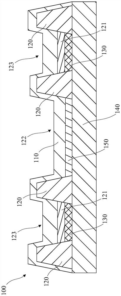
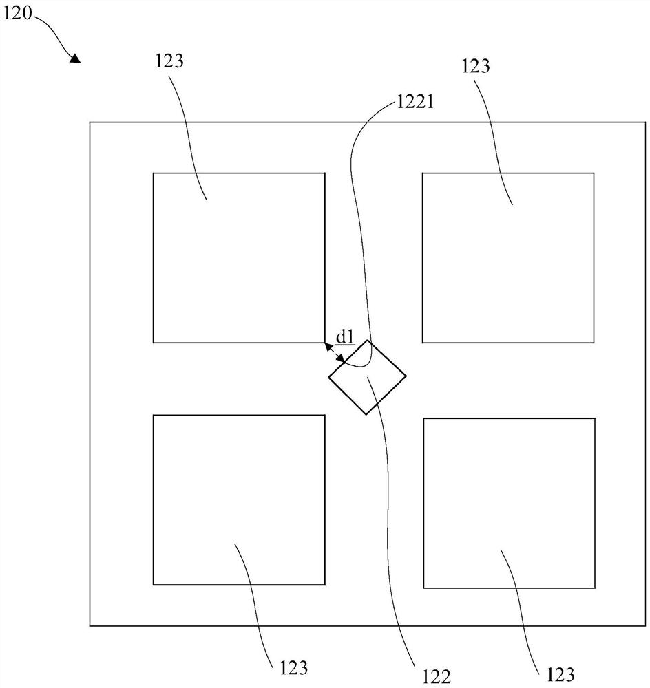
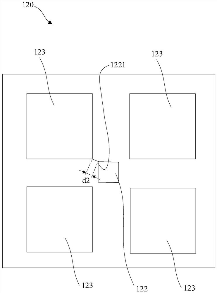
The present application discloses an organic light emitting diode, an OLED display panel and a display device. The organic light emitting diode includes a storage tank layer, and a contact hole and a plurality of storage tanks are opened on the storage tank layer. The storage tanks and the contact holes are arranged at intervals. The contact hole runs through the storage tank layer, and the storage tank is filled with organic light-emitting materials; wherein, the contact hole is provided with a first position point, and the minimum distance between the first position point and the wall surface of the storage tank is the first distance, and the other points of the contact hole The minimum distance between the position and the wall of the storage tank is the second distance, the first distance is smaller than the second distance, and when the contact hole is a polyhedron, the first position point is far away from the edge of the contact hole. In the case that the distance between the storage tank and the center of the contact hole is the same, the minimum distance between the storage tank and the contact hole is increased, thereby preventing the organic light-emitting material in the storage tank from overflowing into the contact hole, ensuring the performance of the organic light emitting diode. Normal display; at the same time, the volume of the filled storage tank can be increased, and the aperture ratio of the organic light-emitting diode can be increased.

Description

technical field [0001] The present application relates to the field of display, and in particular, to an organic light emitting diode, an OLED display panel and a display device. Background technique [0002] With the advancement of technology, organic light-emitting diodes (Organic Light-Emitting Diode, OLED for short) are more and more applied to the display field. A contact hole and a storage tank are arranged in the storage tank layer of the organic light-emitting diode, the organic light-emitting material is printed into the storage tank by an inkjet printing process, and the contact hole is used for connecting the organic light-emitting diode and the lower part of the organic light-emitting diode for A pixel circuit that controls the light emission of an organic light emitting diode. [0003] However, in actual operation, the distance between the storage tank of the organic light-emitting diode and the contact hole is relatively close. During the process of printing t...

Claims


Application Information

Patent Timeline
Patent Type & Authority Patents(China)
IPC IPC(8): H01L51/50H01L51/52H01L27/32
CPCH10K59/38H10K59/122H10K50/00H10K50/80H10K50/8426H10K59/352H10K59/353H10K59/121H10K59/1315H10K71/135H10K50/865
Inventor 许名宏
Owner HEFEI XINSHENG OPTOELECTRONICS TECH CO LTD
Why Eureka
Try Eureka