Interconnection structure and manufacturing method thereof

A manufacturing method and interconnection technology, applied in semiconductor/solid-state device manufacturing, semiconductor/solid-state device components, semiconductor devices, etc., can solve problems such as short circuits, and achieve the effect of improving reliability and increasing overlap margins

Active Publication Date: 2020-11-10
MACRONIX INT CO LTD
View PDF4 Cites 0 Cited by
  • Summary
  • Abstract
  • Description
  • Claims
  • Application Information

AI Technical Summary

Problems solved by technology

In this way, under the condition of high operating voltage, the metal ions in the via window or the conductive layer can easily pass through the dielectric layer and migrate to the adjacent conductive layer (not in direct contact with the via window) to cause a short circuit. question

Method used


Image

  • Interconnection structure and manufacturing method thereof
  • Interconnection structure and manufacturing method thereof
  • Interconnection structure and manufacturing method thereof

Examples


Embodiment Construction

[0040] In order to make the object, technical solution and advantages of the present invention clearer, the present invention will be described in further detail below in conjunction with specific embodiments and with reference to the accompanying drawings.

[0041] The present invention will be described more fully with reference to the accompanying drawings of this embodiment. However, the present invention can also be embodied in various forms and should not be limited to the embodiments described herein. In the drawings, the thicknesses of layers and regions may be exaggerated for clarity. The same or similar reference numerals denote the same or similar elements, and the following paragraphs will not repeat them one by one.

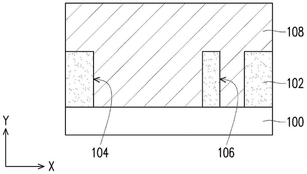
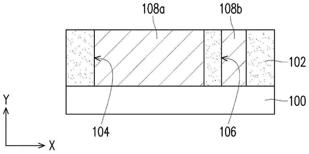
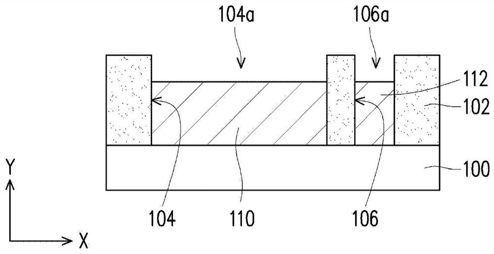
[0042] Figure 1A to Figure 1F It is a schematic cross-sectional view of a method for manufacturing an interconnection structure according to an embodiment of the present invention. figure 2 It is a schematic cross-sectional view of an interconnec...


PUM

PropertyMeasurementUnit
widthaaaaaaaaaa
widthaaaaaaaaaa

Abstract

The invention discloses an intraconnection structure, which comprises a first dielectric layer, a first conductor layer, a second conductor layer, a covering layer and interlayer windows, wherein thefirst dielectric layer has a first channel and a second channel; the first conductor layer is located in the first channel; the second conductor layer is located in the second channel; the top surfaceof the second conductor layer is lower than the top surface of the first dielectric layer; the covering layer covers the first dielectric layer, the first conductor layer and the second conductor layer, and the covering layer is provided with interlayer window openings exposing part of the first conductor layer; the interlayer windows are located on the first conductor layer and the first dielectric layer between the first conductor layer and the second conductor layer; and the interlayer windows fill the interlayer window openings and are electrically connected with the first conductor layer.

Description

technical field [0001] The invention belongs to the field of semiconductor devices, and relates to an internal wiring structure and a manufacturing method thereof. Background technique [0002] With the gradual shrinking of semiconductor components, the overlay window between the upper conductive elements in the interconnection structure and the lower conductive elements below will also become smaller, so misalignment is prone to occur and the reliability of semiconductor components will be reduced. . For example, there are multiple conductive layers in the dielectric layer of the interconnection structure, and the vias are located on the corresponding conductive layers and are electrically connected to them. In addition to the corresponding conductor layer, it also extends to cover the dielectric layer between two adjacent conductor layers. In this way, under the condition of high operating voltage, the metal ions in the via window or the conductive layer can easily pass ...

Claims


Application Information

Patent Timeline
Patent Type & Authority Patents(China)
IPC IPC(8): H01L23/528H01L21/768
CPCH01L21/76802H01L21/76838H01L23/5283
Inventor 黄启豪杨金成
Owner MACRONIX INT CO LTD
Why Eureka
Try Eureka