Package method for printed circuit board (PCB) substrate

A packaging method and substrate technology, applied in the direction of multi-layer circuit manufacturing, etc., can solve the problems of poor positioning accuracy of PCB substrates, achieve stable signal transmission, stable signal transmission, and avoid glue overflow problems

CN103037639AActive Publication Date: 2013-04-10JIANGNAN INST OF COMPUTING TECH
5 Cites 4 Cited by

Patent Information

Authority / Receiving Office
CN · China
Current Assignee / Owner
Publication Date
2013-04-10

Smart Images

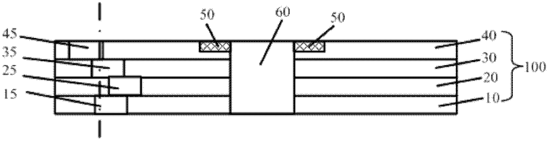
  • Figure 1
    Figure 1
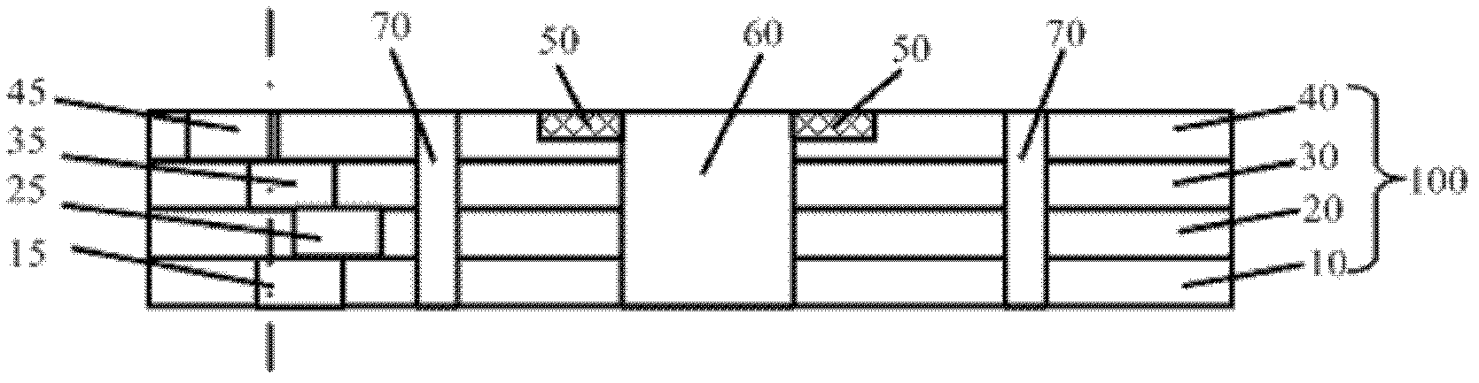
  • Figure 2
    Figure 2
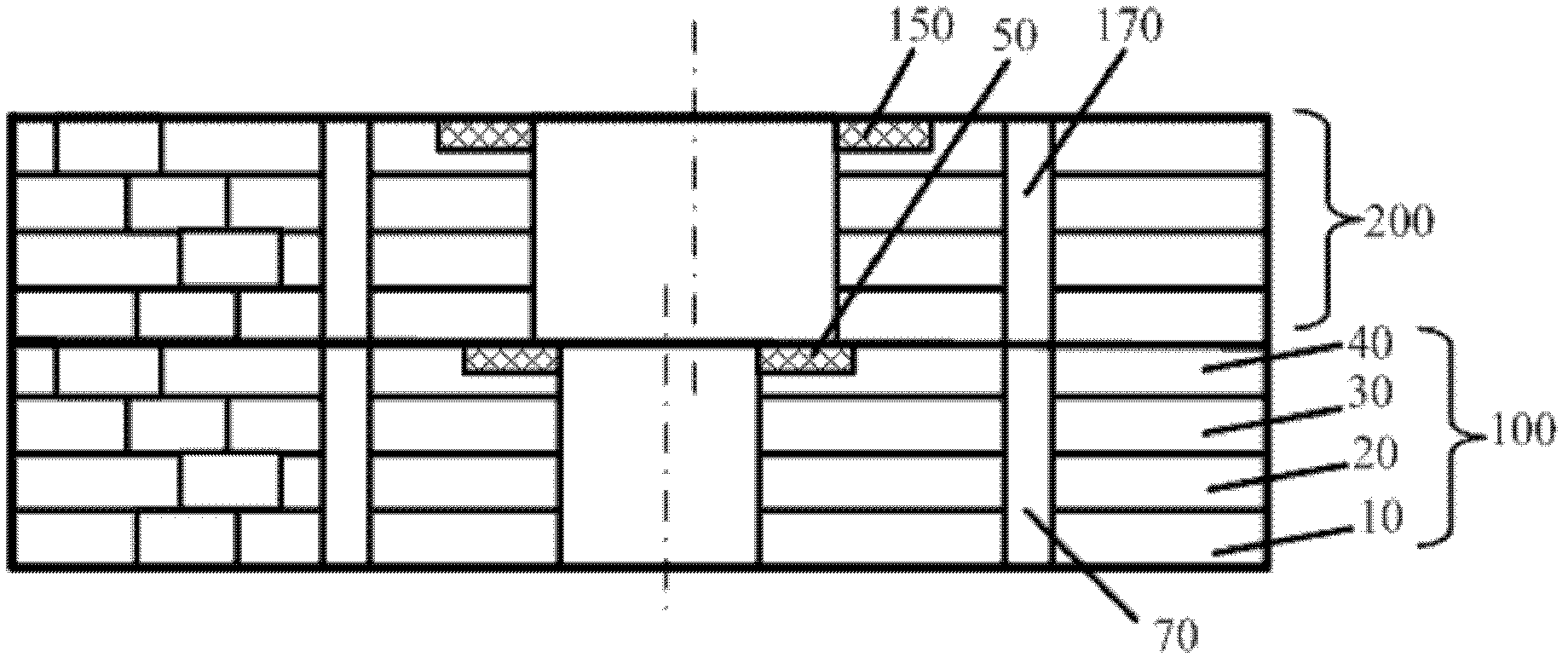
  • Figure 3
    Figure 3
Patent Text Reader

Abstract

A package method for a printed circuit board (PCB) substrate comprises a multilayer plate. The multilayer plate comprises at least two single-layer plates, wherein one single-layer plate is high in counterpoint accuracy requirements, and identification is arranged in the single-layer plate with high counterpoint accuracy requirements. The identification of the single-layer plate, with high counterpoint accuracy requirements, of the multilayer plate is achieved, the center of the identification is calculated, and with the center as a standard, the multilayer plate is drilled at the preset position of a through hole to form the through hole penetrating through all single-layer plates of the multilayer plate. An embodiment of the packing method for the PCB substrate guarantees accuracy of the single-layer plate with high counterpoint accuracy requirement and improves performance of the PCB substrate.
Need to check novelty before this filing date? Find Prior Art

Description

technical field

[0001] The invention relates to the field of manufacturing PCB substrates, in particular to a packaging method for PCB substrates. Background technique

[0002] With the development of science and technology and the advancement of technology, ultra-thin and ultra-light portable electronic products have become the trend and direction of development. Correspondingly, the volume of PCB substrates using these electronic products is becoming smaller and smaller, and the requirements for positioning accuracy of PCB substrates are also getting higher and higher.

[0003] The PCB substrate is usually a multi-layer board. The existing multi-layer board is usually a multi-layer board in which a single-layer board is made first, then the single-layer boards are stacked, and the single-layer boards are pressed together by pressing. In order to facilitate positioning, there is a calibration hole on each single-layer board of the multi-layer board for mechanical alignment...

Examples

Embodiment Construction

[0031] As mentioned in the background art, there are problems in the existing PCB substrate packaging method, resulting in poor alignment accuracy at specific positions of the PCB substrate. The inventors of the embodiments of the present invention found after research that the alignment accuracy of a certain single-layer board among the multi-layer boards of the PCB substrate is often required to be relatively high. Fingers, and if the gold fingers cannot be aligned accurately, it will affect the transmission of signals from the gold fingers to the outside world, and the topmost single-layer board has high requirements for alignment accuracy. Although the overall accuracy of the multi-layer board obtained after drilling with the existing method is improved, when multiple multi-layer boards are stacked, the alignment accuracy of the gold fingers is reduced, which affects the transmission of signals.

[0032] Please refer to image 3 , taking two multi-layer boards as an examp...