
Self-aligned coverage of opaque conductive areas

A transparent conductive, self-aligned process technology, applied in circuits, electrical components, semiconductor devices, etc., can solve the problems of waste of functional areas of light and difficulty in mask coating

Active Publication Date: 2013-04-17
BEIJING XIAOMI MOBILE SOFTWARE CO LTD
View PDF4 Cites 5 Cited by
  • Summary
  • Abstract
  • Description
  • Claims
  • Application Information

AI Technical Summary

Problems solved by technology

Mask coating of printed structures is difficult due to imprecise structures and leads to waste of e.g. light-generating functional areas

Method used


Image

  • Self-aligned coverage of opaque conductive areas
  • Self-aligned coverage of opaque conductive areas
  • Self-aligned coverage of opaque conductive areas

Examples


Embodiment Construction

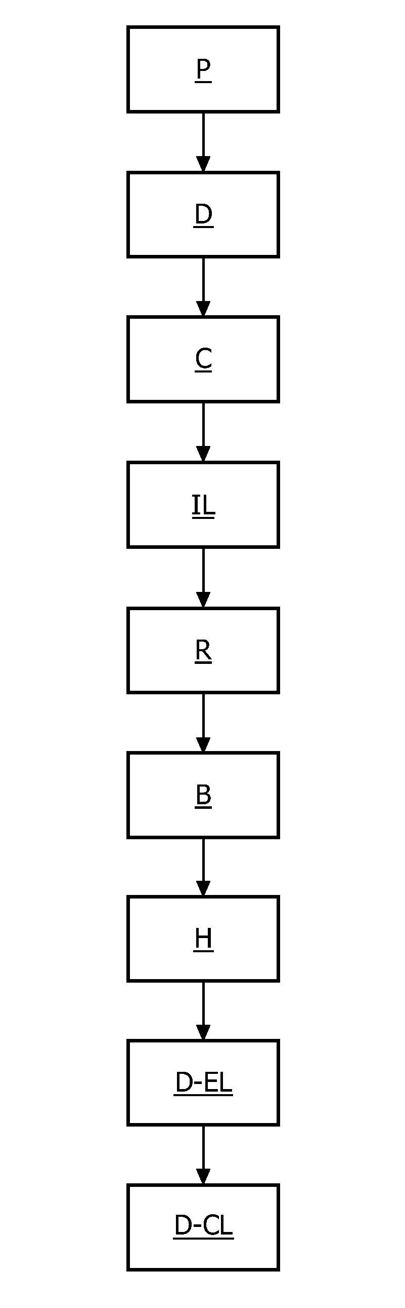
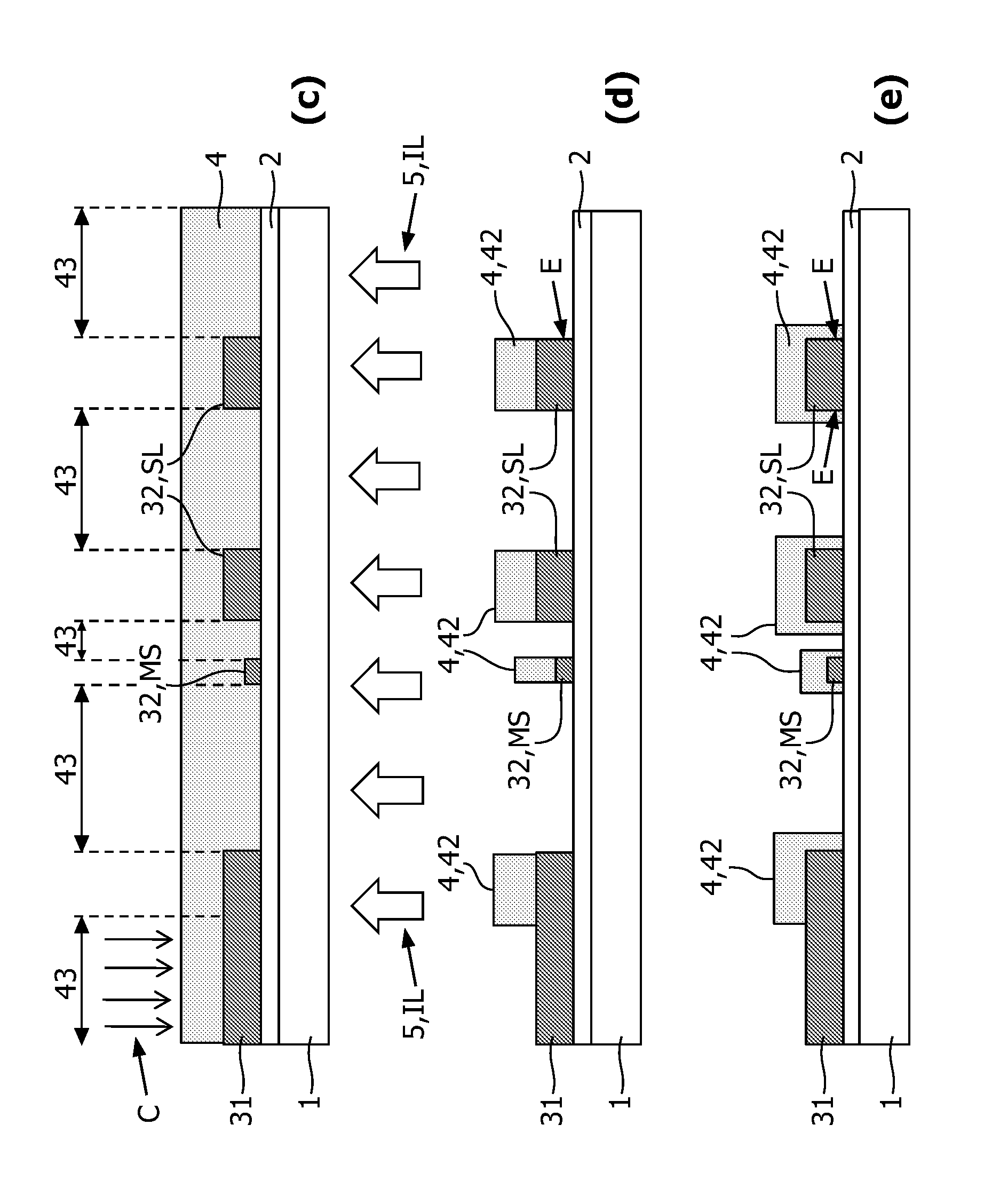
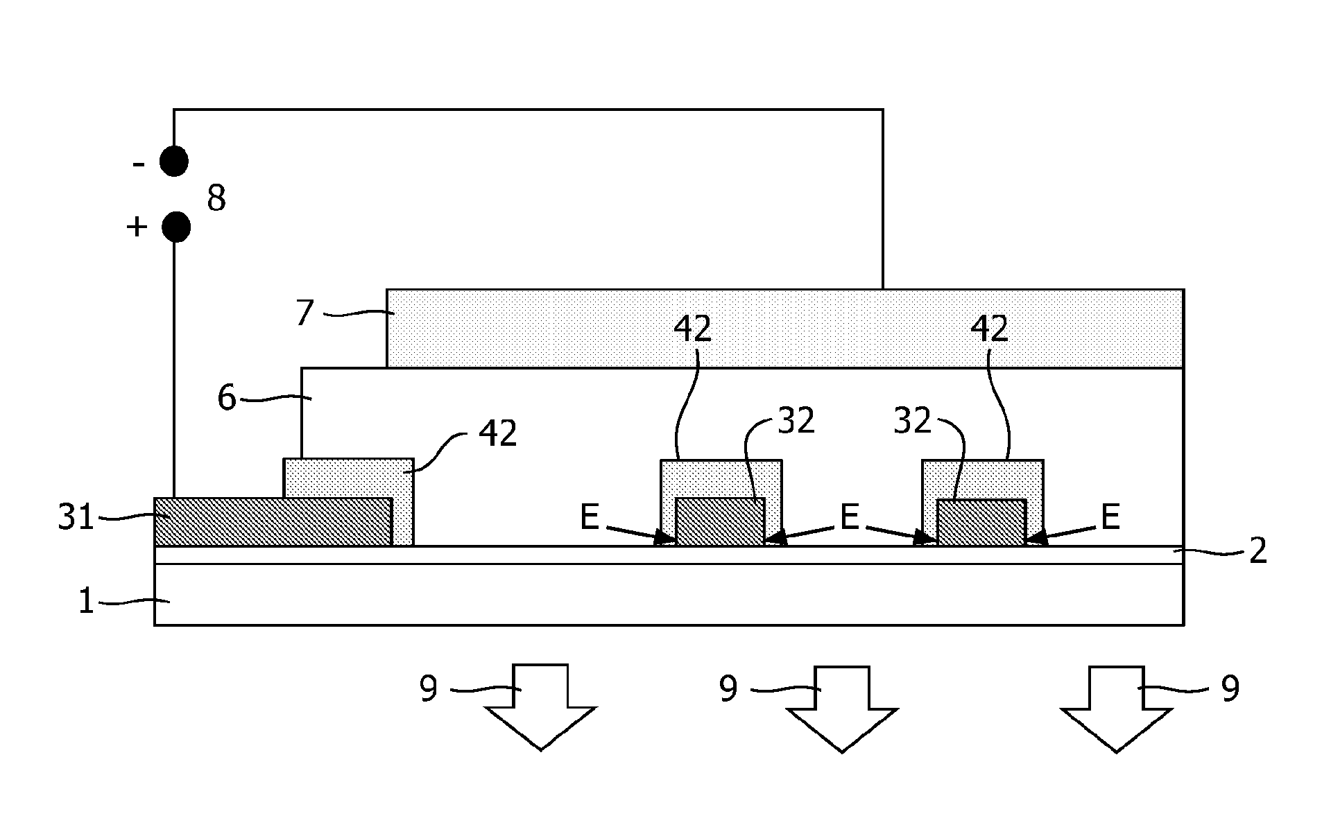
[0032] figure 1 An embodiment of a method according to the invention for covering an opaque conductive area in a self-aligned process is shown, the method comprising process steps (a)-(e), wherein figure 1 (a) shows that the conductive component comprises a substrate 1 , a transparent conductive layer 2 deposited on a transparent substrate 2 with first and second opaque conductive regions 31 , 32 . In this embodiment, the first and second opaque conductive regions are arranged as metal regions, for example as aluminum regions. The first area 31 is arranged as a contact pad for contacting the electrically conductive transparent layer 2 as one of the electrodes of a later completed organic electroluminescent device connected to an external power source to drive the organic electroluminescent device. A typical thickness of such contact pads is 500 nm, the printed silver may have a thickness of 1 μm. The first metal region 31 as this opaque conductive region may be evaporated, p...


PUM


Abstract

The invention relates to a method enabling to apply cheap manufacturing techniques for producing reliable and robust organic thin film device (EL) comprising the steps of providing (P) a transparent substrate (1) at least partly covered with a first layer stack comprising at least one transparent layer (2), preferably an electrically conductive layer, and a pattern of first and second opaque conductive areas (31, 32) deposited on top of the transparent layer (2), depositing (D) a photoresist layer (4) made of an electrically insulating photoresist resist material on top of the first layer stack at least fully covering the second opaque conductive areas (32), illuminating (IL) the photoresist layer (4) through the transparent substrate (1) with light (5) of a suitable wavelength to make the photoresist material soluble in the areas (43) of the photoresist layer (4); having no opaque conductive areas (31, 32) underneath, removing (R) the soluble areas (43) of the photoresist layer (4), heating (B) the areas (42) of the photoresist layer (4) remaining on top of at least the second opaque conductive areas (32) to re-flow the photoresist layer (4) to cover the edges (E) of the second opaque conductive areas (32) in contact to the transparent layer (2), and hardening (H) the remaining areas (42) of the photoresist layer (4). The invention further relates to a conductive component (CC) for use in these organic thin film devices (EL) and to the organic thin film devices (EL) itself.

Description

technical field [0001] The present invention relates to the field of covering opaque conductive regions in a self-alignment process, a method for performing self-alignment covering and an organic thin film device manufactured by this method. Background technique [0002] Organic thin film devices, especially organic electroluminescent devices or organic photovoltaic devices, comprise multiple structured layers, such as electrodes or shunt wires (sometimes also denoted for the grid lines). Existing fabrication processes rely on masked deposition and / or lithographic processes to provide structured layers. The use of masks requires major preparation (each structure requires a separate mask) and process control effort (precise mask-substrate alignment is mandatory) and is therefore a very expensive process. In addition, precise structures also require expensive tools for high-resolution lithography. There is therefore a need to reduce manufacturing costs. Self-aligned deposi...

Claims


Application Information

Patent Timeline
Patent Type & Authority Applications(China)
IPC IPC(8): H01L51/52H10K99/00
CPCH10K50/814H01L21/707H10K2102/301H10K99/00
Inventor S.哈特曼恩C.里克斯H.F.博尔纳H.里夫卡H.施瓦布
Owner BEIJING XIAOMI MOBILE SOFTWARE CO LTD
Learn More