A self-encapsulated mems device and infrared sensor

An infrared sensor, self-encapsulation technology, applied in the direction of piezoelectric devices/electrostrictive devices, piezoelectric/electrostrictive/magnetostrictive devices, instruments, etc., can solve the problem of high packaging requirements, to avoid the packaging process, Reasonable structural features, great commercial value and market effects

Inactive Publication Date: 2015-11-18
PEKING UNIV
View PDF5 Cites 0 Cited by
  • Summary
  • Abstract
  • Description
  • Claims
  • Application Information

AI Technical Summary

Problems solved by technology

In summary, the existing MEMS infrared sensors have very high requirements for packaging

Method used


Image

  • A self-encapsulated mems device and infrared sensor
  • A self-encapsulated mems device and infrared sensor
  • A self-encapsulated mems device and infrared sensor

Examples


Embodiment Construction

[0037] The present invention will be described in detail below through specific embodiments and accompanying drawings.

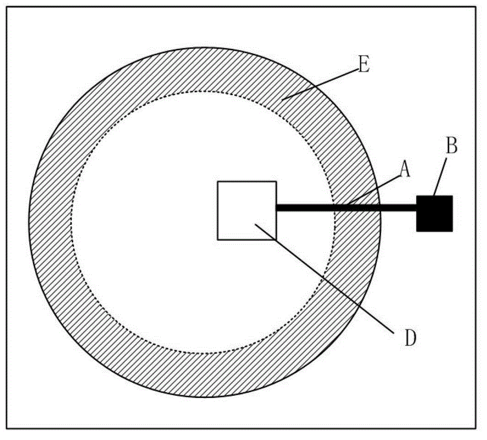
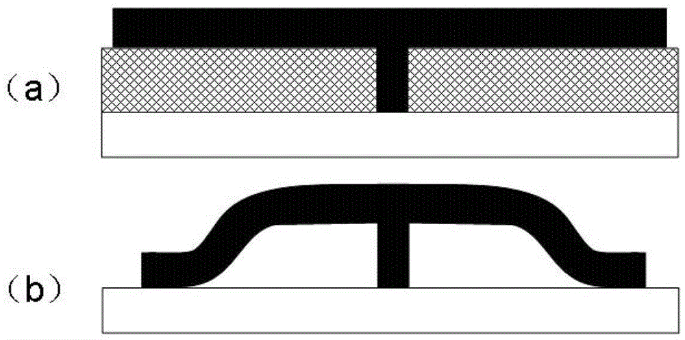
[0038] The infrared chip self-packaging method of the present invention can be applied to MEMS device chips with movable structures processed by surface sacrificial layer integration technology, such as infrared sensors, accelerometers, gyroscopes and other sensors, and actuators such as adjustable capacitance structures. Taking the production of polysilicon / gold dual-material cantilever infrared sensor as an example, the interconnection structure of the capacitive readout method is adopted. The specific process flow is shown in Figure 3, and its description is as follows:

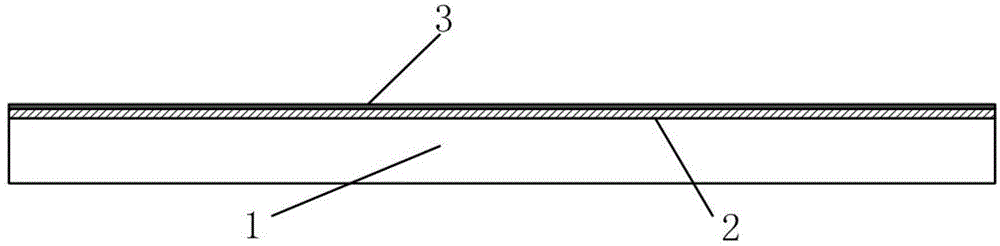
[0039] 1. Preparation sheet: the monocrystalline silicon substrate is used as the substrate 1 of the chip;

[0040] 2. Deposit substrate protection layer, including: LPCVDSiO 2 , with a thickness of 3000 That is, the silicon oxide layer 2 in Figure 3(a) is formed; LPCVDSi 3 N 4 , wi...


PUM


Abstract

The invention discloses a self-packaged MEMS (micro-electro-mechanical systems) device manufactured based on surface sacrificial layer process, and an infrared sensor with the self-packaged MEMS device structure. The self-packaged MEMS device comprises a base plate, a substrate protective layer, a lower electrode, a lower electrode protective layer, a structural layer, a metal layer and a package layer. The structural layer and the metal layer are located in a package chamber formed by the package layer. The package chamber is formed by sticking the package layer onto the lower electrode protective layer according to the adhesion effect when the MEMS device structure is released. The self-packaged MEMS device is applicable to moving-structure MEMS devices such as the infrared sensors. The MEMS device and the package are completed together, so that packaging cycle is shortened and process quality and yield are high. The self-packaged MEMS device is applicable to large-scale batch production.

Description

technical field [0001] The invention belongs to the field of micro-electro-mechanical system (MEMS) processing technology, is particularly applied in the field of MEMS surface sacrificial layer technology, and specifically relates to a self-encapsulated MEMS device based on the surface sacrificial layer technology and an infrared sensor using the device structure. Background technique [0002] Nowadays, MEMS infrared sensors are widely researched and can be applied in scientific and technological fields such as modern technology, national defense and functions. There are many ways to make an infrared sensor. Since the 1990s, microelectromechanical system (MEMS) technology has entered a stage of rapid development, not only because of the novel concept, but also because MEMS devices have the characteristics of miniaturization, integration and better performance compared with traditional devices. Therefore, miniature infrared sensors based on MEMS technology have also been ext...

Claims


Application Information

Patent Timeline
Patent Type & Authority Patents(China)
IPC IPC(8): B81B3/00G01J5/44
Inventor 赵丹淇张大成何军黄贤杨芳田大宇刘鹏王玮李婷罗葵
Owner PEKING UNIV
Why Eureka
Try Eureka