Three-dimensional chip-to-wafer integration

A technology of grain and connection, which is applied in the direction of semiconductor/solid-state device components, semiconductor devices, printed circuits, etc., and can solve problems such as limitations

Active Publication Date: 2013-05-01
MAXIM INTEGRATED PROD INC
View PDF4 Cites 21 Cited by
  • Summary
  • Abstract
  • Description
  • Claims
  • Application Information

AI Technical Summary

Problems solved by technology

However, this type of construction limits the smallest possible spacing between connections to the PCB as determined by the size and spacing requirements of the solder balls

Method used


Image

  • Three-dimensional chip-to-wafer integration
  • Three-dimensional chip-to-wafer integration
  • Three-dimensional chip-to-wafer integration

Examples


Embodiment Construction

[0014] overview

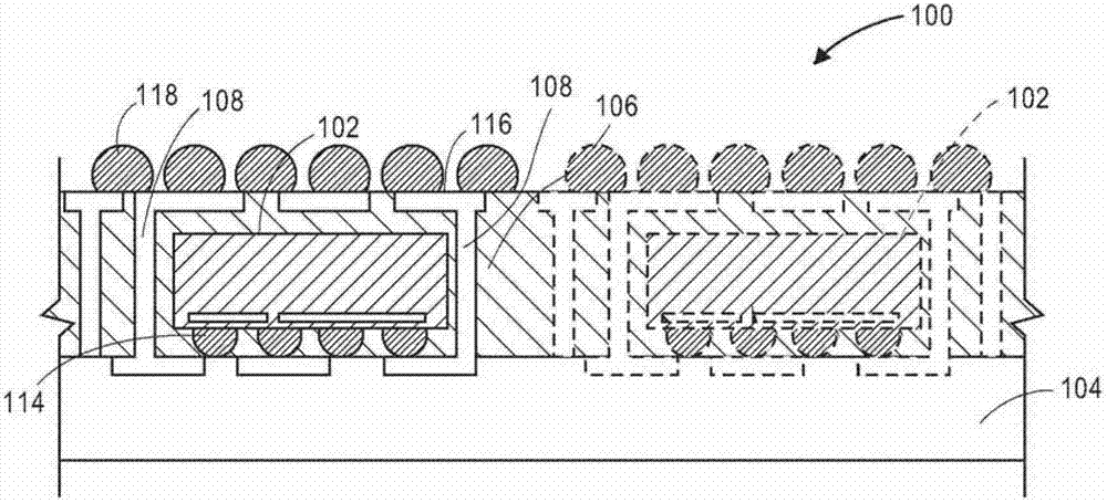
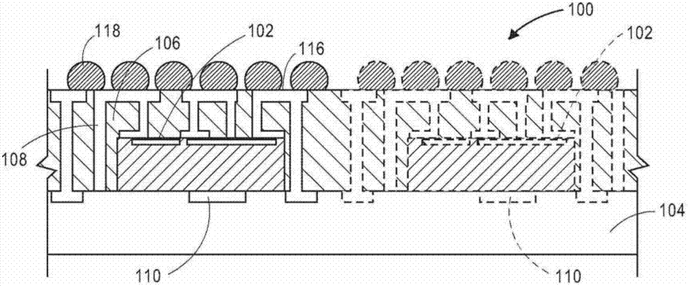
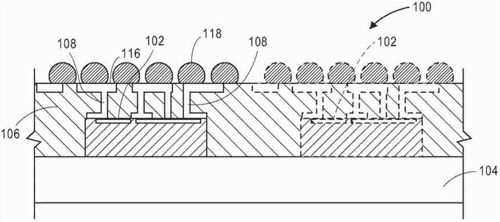
[0015] 3D ICs can be constructed using two or more layers of electronic components integrated into a single IC chip. Electronic components can be stacked to form a single circuit. In some cases, vertical TSVs are used to connect to electronic components of 3D ICs. However, when two or more die are stacked on top of each other, this may require redesigning each die stacked below the other to connect to the underlying die via TSVs. In other cases, through-mold solder connections, such as TMVs, use solder balls to interconnect between the PCB and the top side of the molding compound. However, this type of configuration limits the minimum possible spacing between connections to the PCB as determined by the size of the solder balls and spacing requirements.

[0016] Other types of 3D ICs can be constructed using a molded epoxy wafer on which two or more die are arranged. However, because semiconductor die, such as silicon wafers, have a different coefficient o...


PUM


Abstract

Disclosed is three-dimensional chip-to-wafer integration. An integrated circuit device is disclosed that includes a semiconductor substrate and a die attached to the semiconductor substrate. A conductive pillar is connected to at least one of the semiconductor substrate or the die. An overmold is molded onto the semiconductor substrate over the die, and the conductive pillar extends through the overmold.

Description

Background technique [0001] Three-dimensional integrated circuits (3D ICs) can be constructed with two or more layers of electronic components integrated into a single IC chip. Electronic components can be stacked to form a single circuit. In some cases, vertical through-silicon via (TSV) connections are used to connect to the electronic components of the 3D IC. However, when two or more die are stacked on top of each other, the use of TSV connections may require that each die that is stacked below another die be redesigned to utilize TSV connections to the underlying die. grain. In other cases, through-mold solder connections, such as through-mold via (TMV) connections, use solder balls to provide a connection between the printed circuit board (PCB) and the top side of the mold compound. interconnection. However, this type of configuration limits the smallest possible spacing between connections to the PCB as determined by the size and spacing requirements of the solder b...

Claims


Application Information

Patent Timeline
Patent Type & Authority Applications(China)
IPC IPC(8): H01L23/485H01L23/31H01L21/60H01L21/56
CPCH01L2224/24226H01L25/065H01L24/25H01L23/3121H01L2224/97H01L24/73H01L2224/24146H01L2924/01029H01L2224/25171H01L24/19H05K1/185H01L24/24H01L2224/02371H01L2224/94H01L2224/73209H01L21/56H01L2224/96H01L2224/73267H01L23/485H01L2224/05548H01L2224/0239H01L23/49811H01L2224/13024H01L23/31H01L21/561H01L24/16H01L2224/16225H01L2924/10253H01L23/5389H01L2224/12105H01L2224/131H01L2224/16145H01L2224/16227H01L2224/32145H01L2224/73253H01L2225/06586H01L25/50H01L2225/06513H01L2225/06558H01L2225/06524H01L2924/1461H01L2224/0401H01L2924/181H01L2924/3511H01L25/0657H01L2224/11H01L2924/00014H01L2924/01079H01L2224/81H01L2924/00H01L2924/014H01L2225/06548H01L2225/06589
Inventor A·S·科尔卡K·坦比杜赖V·汉德卡尔H·D·阮
Owner MAXIM INTEGRATED PROD INC
Why Eureka
Try Eureka