Preparation method of display panel

A substrate and color filter substrate technology, applied in nonlinear optics, instruments, optics, etc., can solve the problem of uneven film thickness and wide area, and achieve the effect of high practical application value in production

Inactive Publication Date: 2013-05-08
HEFEI BOE OPTOELECTRONICS TECH +1
View PDF4 Cites 10 Cited by
  • Summary
  • Abstract
  • Description
  • Claims
  • Application Information

AI Technical Summary

Problems solved by technology

[0010] The embodiment of the present invention provides a method for manufacturing a display panel, which is used to solve the problem that the film thickness uneven area is relatively wide when the alignment film of the display panel is manufactured by inkjet printing in the prior art

Method used


Image

  • Preparation method of display panel
  • Preparation method of display panel
  • Preparation method of display panel

Examples


Embodiment Construction

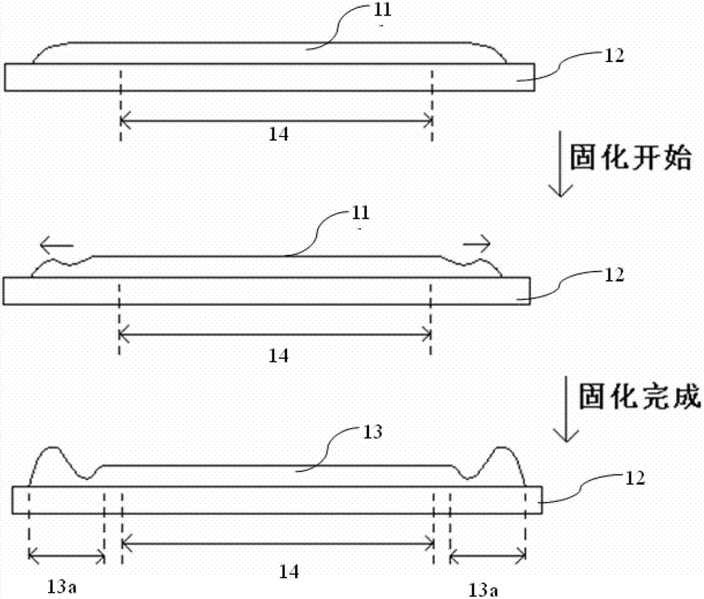
[0023] An embodiment of the present invention provides a method for manufacturing a display panel, which is used to solve the problem of relatively wide areas of uneven film thickness when an alignment film of a display panel is manufactured by inkjet printing in the prior art.

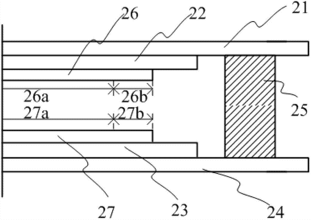
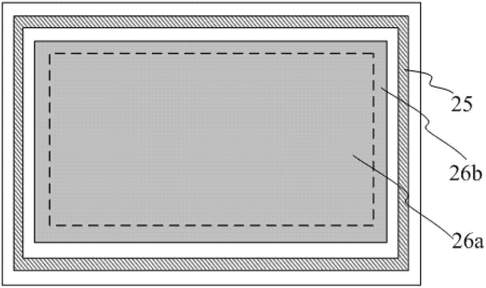
[0024] An embodiment of the present invention provides a method for manufacturing a display panel, wherein the structure of the display panel is as follows figure 2 as shown, figure 2 For the sectional view of the display panel, from figure 2 It can be seen from the figure that the display panel includes a color filter side substrate 21, a color filter substrate substrate 22, a thin film transistor substrate substrate 23, an array side substrate 24, and a sealant 25, and the display panel also includes a first alignment film 26 and a second alignment film 27, the first alignment film 26 is located under the color filter substrate substrate 22, facing the side of the array side substrate 24, the se...


PUM


Abstract

The invention discloses a preparation method of a display panel. The preparation method of the display panel is used for solving the problem in the prior art that an area where the thickness of film is uneven is wide when an ink jet type printing mode is adopted to manufacture alignment film of the display panel. The preparation method of the display panel comprises manufacturing a color film substrate underlay on one side, facing an array side substrate, of the lower portion of a color film substrate; manufacturing a film even-thickness area and a film uneven-thickness area of first alignment film below the color film substrate underlay by using different temperatures of solidification or alignment liquid with different viscosity; manufacturing a thin film transistor substrate underlay on one side, facing the color film side substrate, on the upper portion of the array side substrate; and manufacturing a film even-thickness area and a film uneven-thickness area of second alignment film on the thin film transistor substrate underlay by using different temperatures of solidification or alignment liquid with different viscosity.

Description

technical field [0001] The invention relates to the technical field of liquid crystal display, in particular to a method for manufacturing a display panel. Background technique [0002] Liquid crystal panel display is currently the mainstream flat panel display, widely used in televisions, notebooks, digital cameras, mobile handheld devices and other fields. [0003] In the liquid crystal display panel, in order to make the liquid crystal molecules form a certain orientation, it is necessary to make an alignment film on both sides of the color filter side substrate and the array side substrate in the liquid crystal panel display, and the material of the alignment film is polyimide film (Polyimide Film) , referred to as PI). [0004] However, if figure 1 It is shown that due to the influence of external factors, it is inevitable to form a region with uneven film thickness in the edge region of the alignment film during the process of making the alignment film. The reasons a...

Claims


Application Information

Patent Timeline
Patent Type & Authority Applications(China)
IPC IPC(8): G02F1/1337G02F1/1333
Inventor 申莹涂志中尹傛俊
Owner HEFEI BOE OPTOELECTRONICS TECH
Why Eureka
Try Eureka