Array substrate, drive method of array substrate and display device of array substrate

An array substrate, driving signal technology, applied in static indicators, instruments, semiconductor devices, etc., can solve the problems of product yield impact, line length, large resistance differences, etc., to avoid bad horizontal lines, reduce the number of wiring, reduce The effect of resistance differences

Active Publication Date: 2013-05-08
BEIJING BOE OPTOELECTRONCIS TECH CO LTD
View PDF6 Cites 8 Cited by
  • Summary
  • Abstract
  • Description
  • Claims
  • Application Information

AI Technical Summary

Problems solved by technology

The disadvantage of the array substrate with such a structure is that the lines around the pixel unit 13 are usually long, and there will be relatively large resistance differences between metals of different layers, especially for gate lines with thinner line widths. , the overall resistance difference between two adjacent rows of gate lines is relatively large, and it is easy to show differences between rows during the display process of the display device, resulting in poor horizontal lines (H-line), which is harmful to the product has a great influence on the yield of

Method used


Image

  • Array substrate, drive method of array substrate and display device of array substrate
  • Array substrate, drive method of array substrate and display device of array substrate
  • Array substrate, drive method of array substrate and display device of array substrate

Examples


Embodiment Construction

[0025] The following will clearly and completely describe the technical solutions in the embodiments of the present invention with reference to the accompanying drawings in the embodiments of the present invention. Obviously, the described embodiments are only some, not all, embodiments of the present invention. All other embodiments obtained by persons of ordinary skill in the art based on the embodiments of the present invention belong to the protection scope of the present invention.

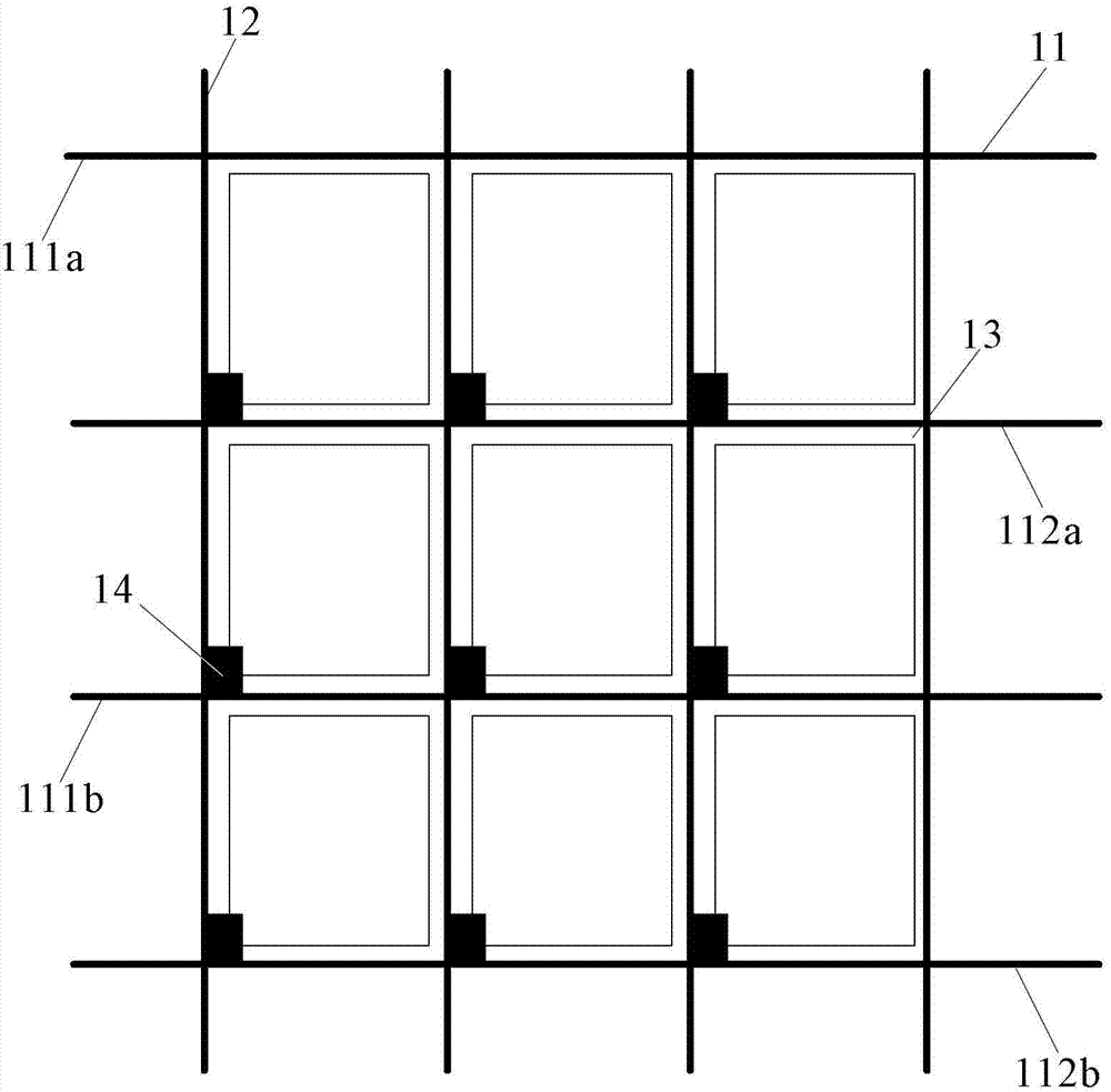
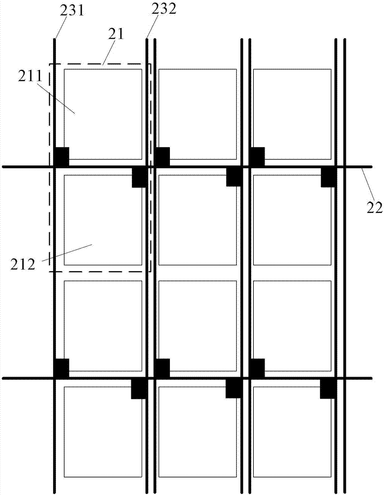
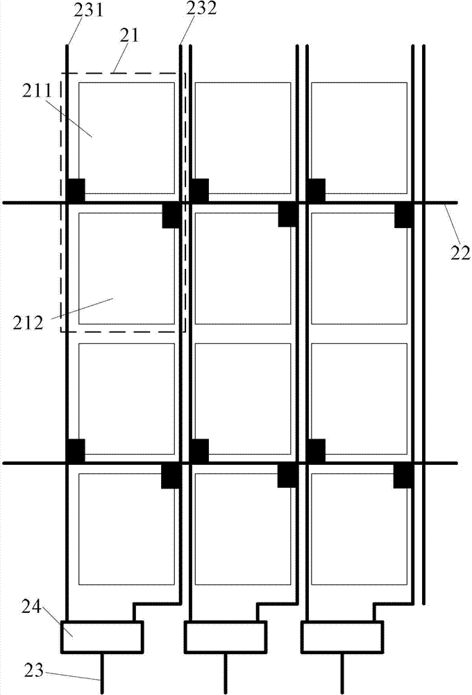
[0026] The array substrate provided by the embodiment of the present invention, such as figure 2 As shown, it includes: a plurality of pixel groups 21 arranged in a matrix, a plurality of rows of gate lines 22 arranged horizontally corresponding to each pixel group 21, a plurality of columns of first data lines 231 and a plurality of columns of second data lines 232 arranged in a vertical direction .

[0027] Each pixel group 21 includes a first pixel unit 211 and a second pixel unit 212 , ...


PUM


Abstract

The invention provides an array substrate, a drive method of the array substrate and a display device of the array substrate, and relates to the technical field of display. The array substrate, the drive method of the array substrate and the display device of the array substrate are capable of avoiding that a horizontal line is poor, and improving yield of products of the display device of the array substrate. The array substrate comprises a plurality of pixel groups which are arranged in an matrix mode, a plurality of grid lines which correspond to the pixel groups and are transversely arranged, a plurality of columns of first data lines and a plurality of columns of second data lines, wherein the first data lines and the second data lines are lengthways arranged. Each pixel group comprises a first pixel unit and a second pixel unit. The first pixel unit and the second pixel unit are arranged on two adjacent lines. A grid line is respectively connected with a first pixel unit and a second pixel unit in a corresponding pixel group. A first data line is connected with the first pixel unit of the corresponding pixel group so as to provide data signals for the first pixel unit. A second data line is connected with the second pixel unit of the corresponding pixel group so as to provide data signals for the second pixel unit. The grid lines on the periphery of pixel units are formed by the same layer of metal.

Description

technical field [0001] The present invention relates to the field of display technology, in particular to an array substrate, a driving method thereof, and a display device. Background technique [0002] At present, narrow bezel display devices have gradually become the mainstream of display product development. The key to obtaining a display device with narrower bezels is to reduce the range of gate lines or data line circuits located around the display area in the array substrate. [0003] The existing array substrate can be as figure 1 As shown, it includes a plurality of pixel units 13 divided by crossing gate lines 11 and data lines 12, each pixel unit 13 has a TFT (Thin Film Transistor, thin film transistor) region 14, gate lines 11 and data lines 12 The pixel unit 13 is driven to work by the TFT in the TFT region 14 . In the existing array substrate, the gate lines located inside the region where the pixel unit 13 is located can all be formed of the same layer of me...

Claims


Application Information

Patent Timeline
Patent Type & Authority Applications(China)
IPC IPC(8): G02F1/1362G02F1/1368G02F1/133G09G3/36
CPCG09G2300/0465G09G3/20G09G3/3659G09G3/2085G09G2320/0223H01L27/124G09G2310/0218G09G3/3648G09G2300/0426
Inventor 李月薛艳娜王磊
Owner BEIJING BOE OPTOELECTRONCIS TECH CO LTD
Why Eureka
Try Eureka