Touch panel and touch display with same
A touch display and touch panel technology, applied in the input/output process of instruments, data processing, electrical digital data processing, etc., can solve problems such as surface fogging and light reflection
- Summary
- Abstract
- Description
- Claims
- Application Information
AI Technical Summary
Problems solved by technology
Method used
Image

Examples
no. 1 example
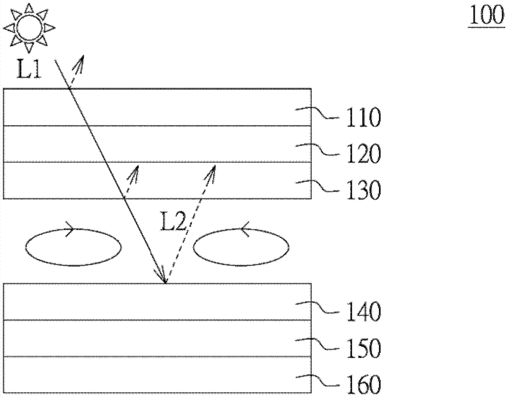
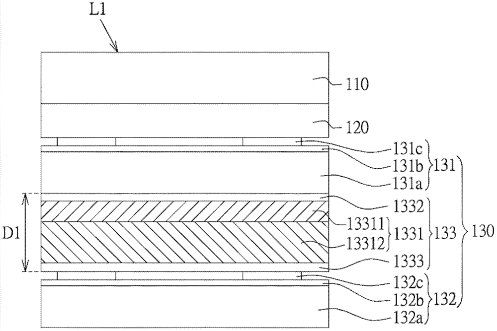
[0042] Please refer to figure 1 , which shows a schematic diagram of the touch display 100 . The touch display 100 includes a transparent protection plate 110 , a display panel 150 and a touch panel 130 . The transparent protection plate 110 is used to protect the touch display 100 to prevent the touch display 100 from getting wet, scratched or impacted. The display panel 150 is used to display a picture, such as a liquid crystal display panel (LCD Display), an organic light emitting diode panel (OLED Display) or an electronic paper display panel (Electronic Paper Display). In the touch display 100 shown in this schematic diagram, the display panel 150 is illustrated by taking a liquid crystal display panel as an example. The touch panel 130 is used for sensing signals touched by the user, for example, a capacitive touch panel or an electromagnetic induction touch panel.
[0043] The touch panel 130 is disposed between the transparent protection plate 110 and the display pa...
no. 2 example
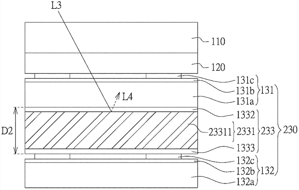
[0052] Please refer to image 3 , which shows an enlarged schematic view of the transparent protective plate 110 , the optically clear adhesive (OCA) 120 and the touch panel 230 of the second embodiment. The difference between the touch panel 230 of this embodiment and the touch panel 130 of the first embodiment lies in the optical adjustment film 233 , and the rest of the similarities will not be described again.
[0053] Such as image 3 As shown, the optical adjustment layer 2331 of the optical adjustment film 233 includes an anti-reflection layer (anti-reflection layer) 23311 , such as a multilayer refraction material structure, a graded refraction material structure or a moth-eye structure. When external light enters the touch panel 230 and passes through the anti-reflection layer 23311 , most of the external light will be refracted inside due to the characteristics of the anti-reflection layer 23311 , so that the reflection phenomenon will be greatly reduced.
[0054] ...
no. 3 example
[0057] Please refer to Figure 4 , which shows an enlarged schematic view of the transparent protective plate 110 , the optically clear adhesive (OCA) 120 and the touch panel 330 of the third embodiment. The difference between the touch panel 330 of this embodiment and the touch panel 130 of the first embodiment lies in the optical adjustment film 333 , and the rest of the similarities will not be described again.
[0058] Such as Figure 4 As shown, the optical adjustment layer 3331 of the optical adjustment film 333 includes an anti-fogging layer 33311 . Due to the characteristics of the anti-fogging layer 33311, when the temperature changes or the user touches it with fingers, it is not easy to cause fogging.
[0059] In addition, the conductivity of the anti-fogging layer 33311 of the optical adjustment film 333 is lower than 10. -8 S / cm. That is to say, the optical adjustment film 333 of this embodiment also has good insulation, which can well isolate the first transp...
PUM
 Abstract
Description
Claims
Application Information
 - R&D Engineer
- R&D Manager
- IP Professional
- Industry Leading Data Capabilities
- Powerful AI technology
- Patent DNA Extraction
Browse by: Latest US Patents, China's latest patents, Technical Efficacy Thesaurus, Application Domain, Technology Topic.
© 2024 PatSnap. All rights reserved.Legal|Privacy policy|Modern Slavery Act Transparency Statement|Sitemap