A double-sided perc solar cell structure and its preparation process
A technology for solar cells and fabrication processes, applied in sustainable manufacturing/processing, circuits, electrical components, etc., can solve problems that affect the front conversion efficiency of cells, increase the LID and PID risks of cells and components, and achieve bifacial ratio and Improved anti-LID effect, double-sided ratio and anti-LID effect, improved anti-reflection effect
- Summary
- Abstract
- Description
- Claims
- Application Information
AI Technical Summary
Problems solved by technology
Method used
Image
Examples
Embodiment 1
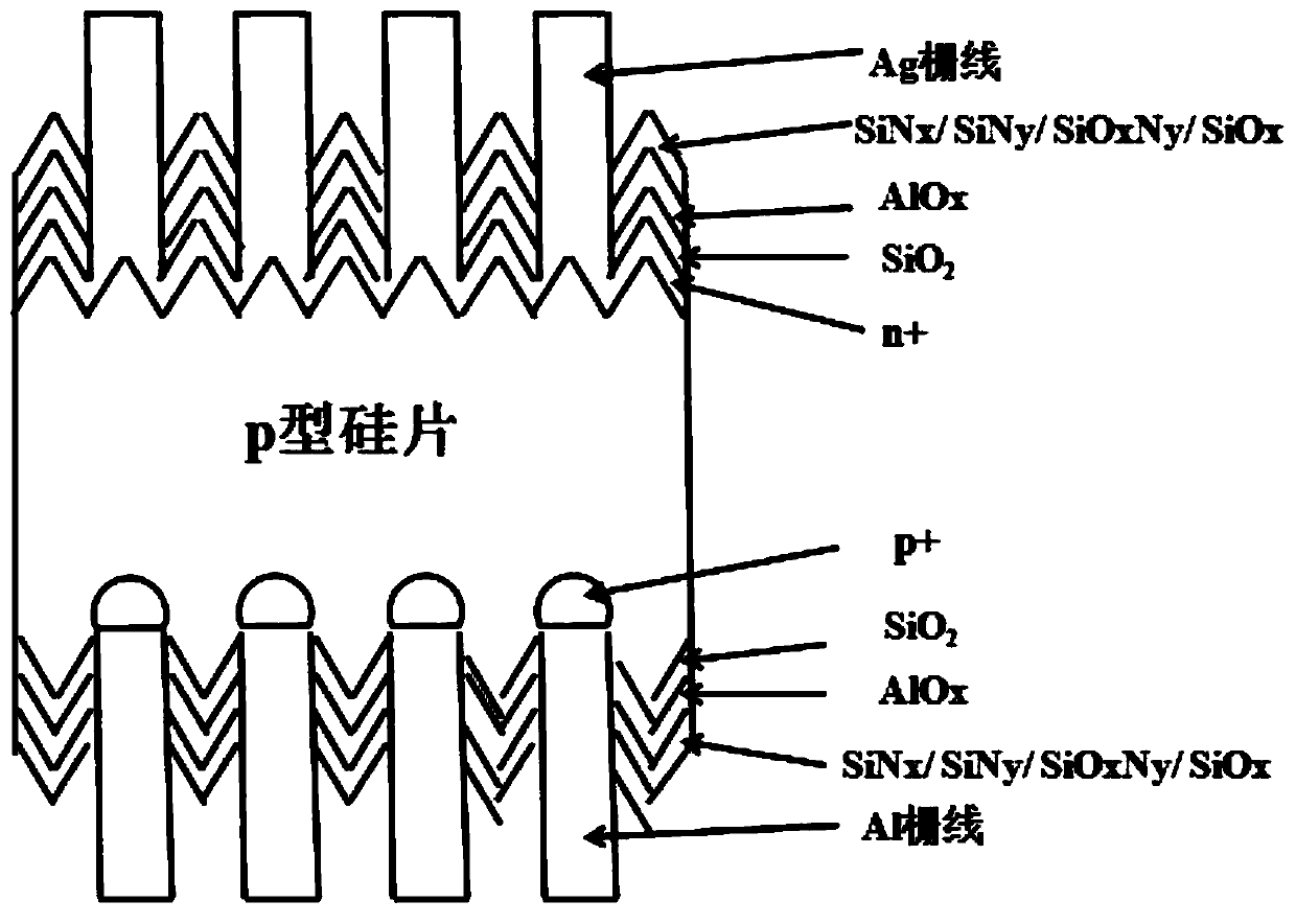
[0028] refer to figure 1 , a bifacial PERC solar cell structure with SiO on the front and back of the cell 2 / AlOx / SiNx / SiNy / SiOxNy / SiOx stacked structure, where the front and back SiO 2 layer is simultaneously formed by thermal oxidation or ozone oxidation, SiO 2 Layer thickness 5-20nm; front and back AlOx(Al 2 o 3 ) layer is formed by simultaneous deposition of atomic layer deposition (ALD), the AlOx layer thickness is 3-30nm, and the refractive index is 1.60-1.65; or a combination of two or more) are formed by PECVD deposition respectively, the thickness of the front SiNx / SiNy / SiOxNy / SiOx stack is 5-20nm, 20-40nm, 30-50nm and 40-60nm respectively, and the total thickness of the stack is 80-90nm , the refractive indices are 2.0-2.3, 1.8-2.0, 1.6-1.9 and 1.4-1.6 respectively; the backside SiNx / SiNy / SiOxNy / SiOx stack thicknesses are 15-30nm, 30-60nm, 40-70nm and 60-90nm respectively, The total thickness of the stack is 80-160nm, and the refractive indices are 2.0-2.3, 1.8...
Embodiment 2
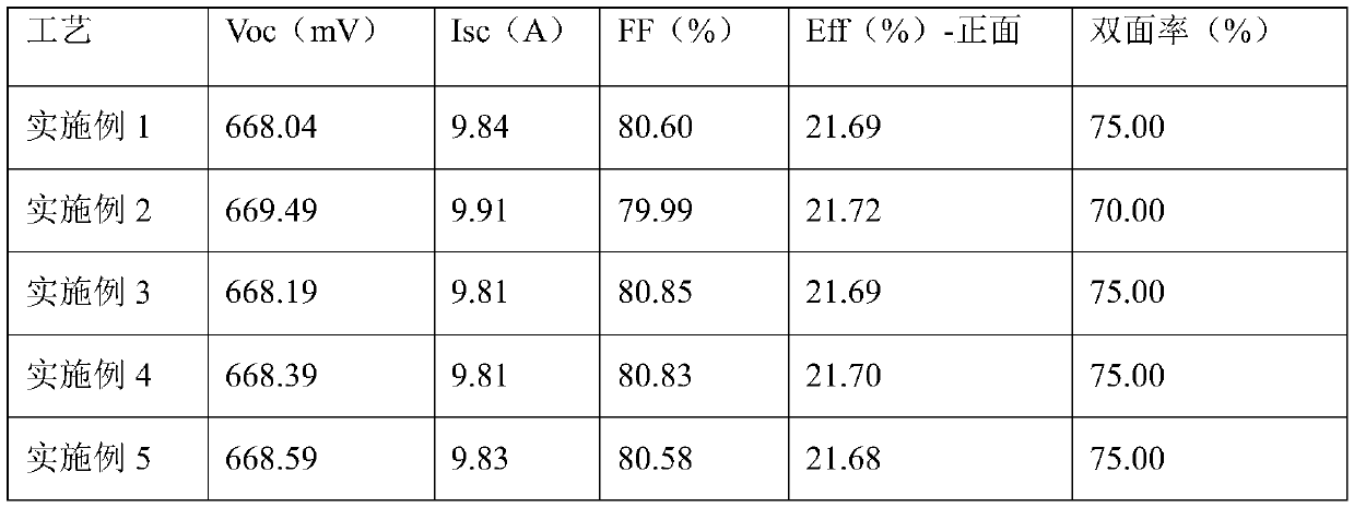
[0040] In the third step of embodiment 1, the belt speed of back chain etching is 1.5m / min, the etching depth is 5um, and the reflectivity of the back surface is 40%; other processes are the same as in embodiment 1.
Embodiment 3
[0042] In the 5th step in embodiment 1, ALD deposits, deposits Al simultaneously on both sides 2 o 3 , the deposition temperature is 250° C., the pressure is 100 mTor, and the time is 400 s; other processes are the same as in Example 1.
PUM
| Property | Measurement | Unit |
|---|---|---|
| thickness | aaaaa | aaaaa |
| refractive index | aaaaa | aaaaa |
| thickness | aaaaa | aaaaa |
Abstract
Description
Claims
Application Information


