Printed circuit board and manufacture method thereof

A printed circuit board and manufacturing method technology, which is applied in the directions of printed circuit components, the formation of electrical connection of printed components, and the electrical connection of printed components, etc., can solve the problems of calculating impedance value and inability, and achieve continuous via impedance and improve signal integrity. sexual effect

Inactive Publication Date: 2013-05-08
INVENTEC PUDONG TECH CORPOARTION +1
View PDF3 Cites 11 Cited by
  • Summary
  • Abstract
  • Description
  • Claims
  • Application Information

AI Technical Summary

Benefits of technology

The technical effect that this new design allows for better electrical performance when used with electronic devices such as computers or communication equipment. It also provides an improved way to connect signals between different layers within the device's substrate layer without adding extra components like wires.

Problems solved by technology

This patent describes two main challenges faced during the development process of electronic components: signal communication issues and signal quality degradation. These factors affecting signal integrity require careful consideration while ensuring proper performance of these circuits.

Method used


Image

  • Printed circuit board and manufacture method thereof
  • Printed circuit board and manufacture method thereof
  • Printed circuit board and manufacture method thereof

Examples


Embodiment Construction

[0023] The following is a detailed description of the embodiments in conjunction with the accompanying drawings, but the provided embodiments are not used to limit the scope of the present invention, and the description of the structure and operation is not used to limit the order of its execution, and any recombination of components The structure of the resulting device with equal efficacy is within the scope of the present invention. In addition, the drawings are for illustrative purposes only and are not drawn to original scale.

[0024] As used herein, "about", "approximately" or "approximately" generally means that the error or range of the value is within 20 percent, preferably within 10 percent, and more preferably It is within five percent. If there is no explicit statement in the text, the numerical values ​​mentioned are regarded as approximate values, that is, the error or range indicated by "about", "approximately" or "approximately".

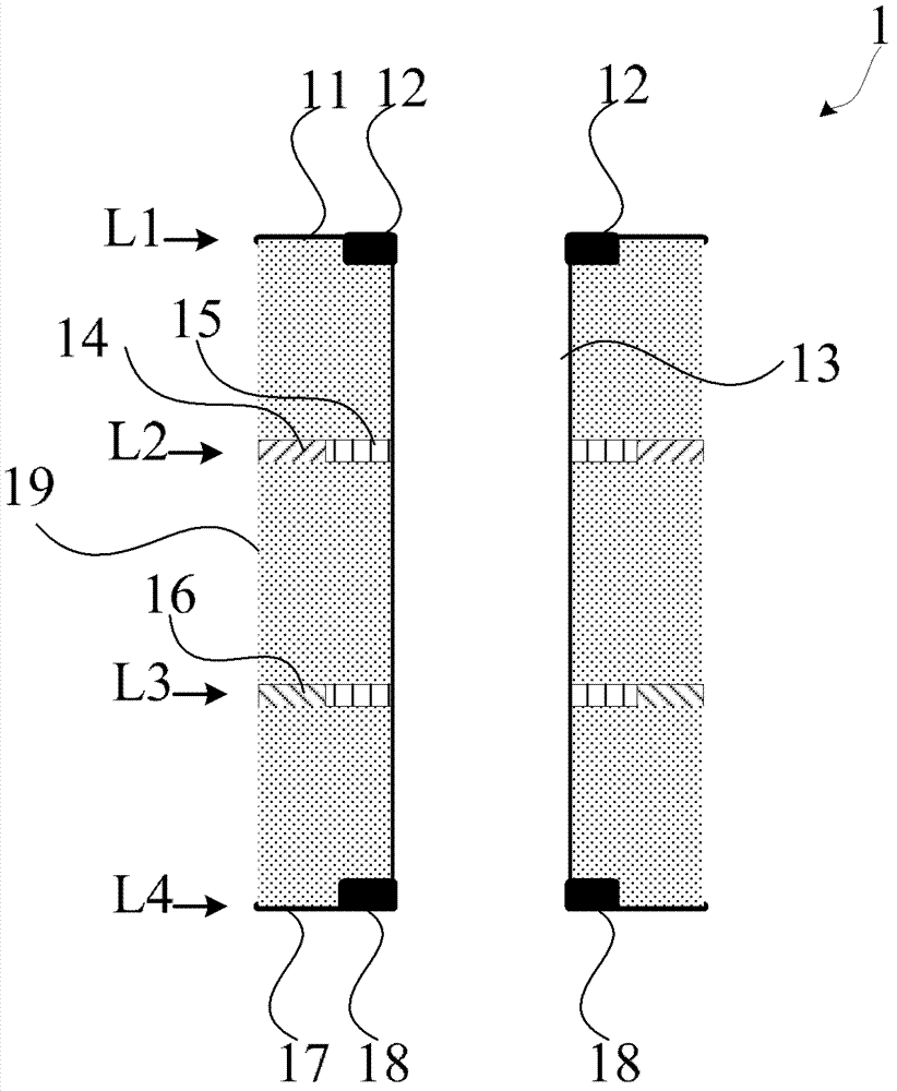
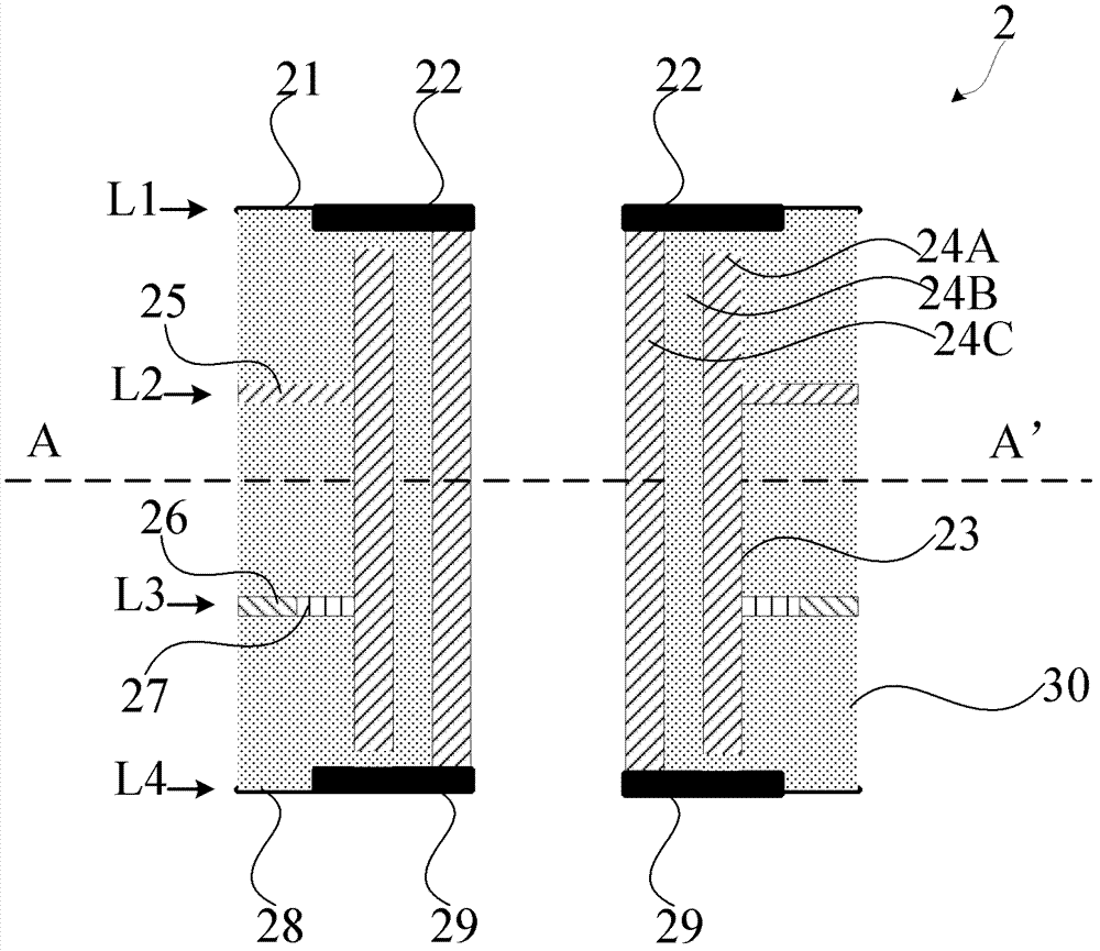
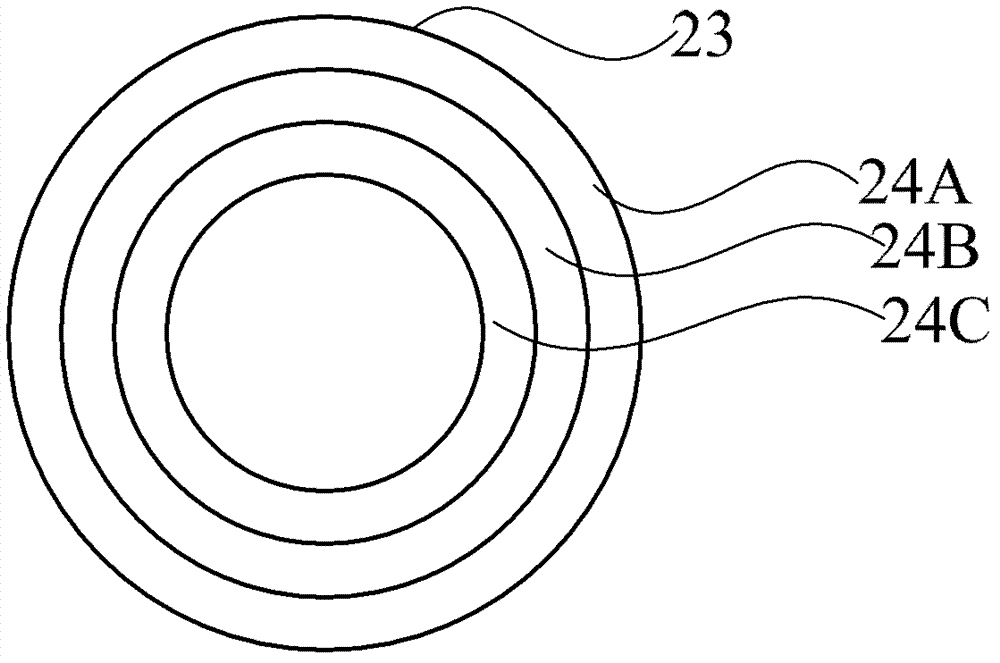
[0025] Please refer to f...


PUM


Abstract

The invention provides a printed circuit board and a manufacture method of the printed circuit board. The printed circuit board comprises a first wiring layer, a second wiring layer, a first plane layer and a second plane layer, wherein the first plane layer and the second plane layer are arranged between the first wiring layer and the second wiring layer. The printed circuit board further comprises a penetrating hole structure which penetrates through the first wiring layer, the first plane layer, the second plane layer and the second wiring layer. The penetrating hole structure comprises a through hole, a first conductor layer arranged on the inner wall of the through hole, a first insulating layer arranged on the ring surface of the first conductor layer, and a second conductor layer arranged on the ring surface of the first insulating layer, wherein the first conductor layer is electrically connected with the first plane layer or the second plane layer, and is connected with the first wiring layer and the second wiring layer in an electric insulation mode, and the second conductor layer is electrically connected with the first wiring layer and the second wiring layer, and serves as a signal carrier to transmit a signal produced by the first wiring layer to the second wiring layer.

Description


Claims


Application Information

Patent Timeline
Owner INVENTEC PUDONG TECH CORPOARTION
Why Eureka
Try Eureka