Voltage biased section of non-linear transmission line

a nonlinear transmission line and voltage biasing technology, applied in pulse generators, high frequency circuit adaptations, pulse techniques, etc., can solve the problems of demuxinig contributing greatly to the complexity of electro-optic and processing/switching modules and the routing density of pcbs, the standard back plane and other electrical connectors possess too high parasitic inductance, capacitance, resistance and conductance. , to achieve the effect of reducing stub effects and reducing stub effects

Inactive Publication Date: 2003-03-25
RPX CLEARINGHOUSE
View PDF11 Cites 33 Cited by
  • Summary
  • Abstract
  • Description
  • Claims
  • Application Information

AI Technical Summary

Benefits of technology

Preferably a resistor is connected in series with said voltage such that the distance between the resistor and the first part is less than the distance between the voltage and the fi

Problems solved by technology

This level of demuxinig contributes greatly to the complexity of the electro-optic and processing/switching modules and the routing density on the PCBs.
In addition, the power requirements of the demux and mux units can be significant.
The principal reason that commercially available 10 gigabits per second electrical interconnect has not previously been achieved is that the standard back plane and other electrical connectors possess too high a level of parasitic inductance, capacitance, resistance and conductance.
In addition, the PCBs themselves may introduce prohibitive levels of attenuation due to frequency-dependent track resistance and dielectric substrate conductance.
These result in attenuation, harmonic distortion and dispersion (to name a few) to an extent that makes sufficiently error-free transmission of

Method used


Image

  • Voltage biased section of non-linear transmission line
  • Voltage biased section of non-linear transmission line
  • Voltage biased section of non-linear transmission line

Examples


Embodiment Construction

Embodiments of the present invention are described below by way of example only. These examples represent the best ways of putting the invention into practice that are currently known to the Applicant although they are not the only ways in which this could be achieved.

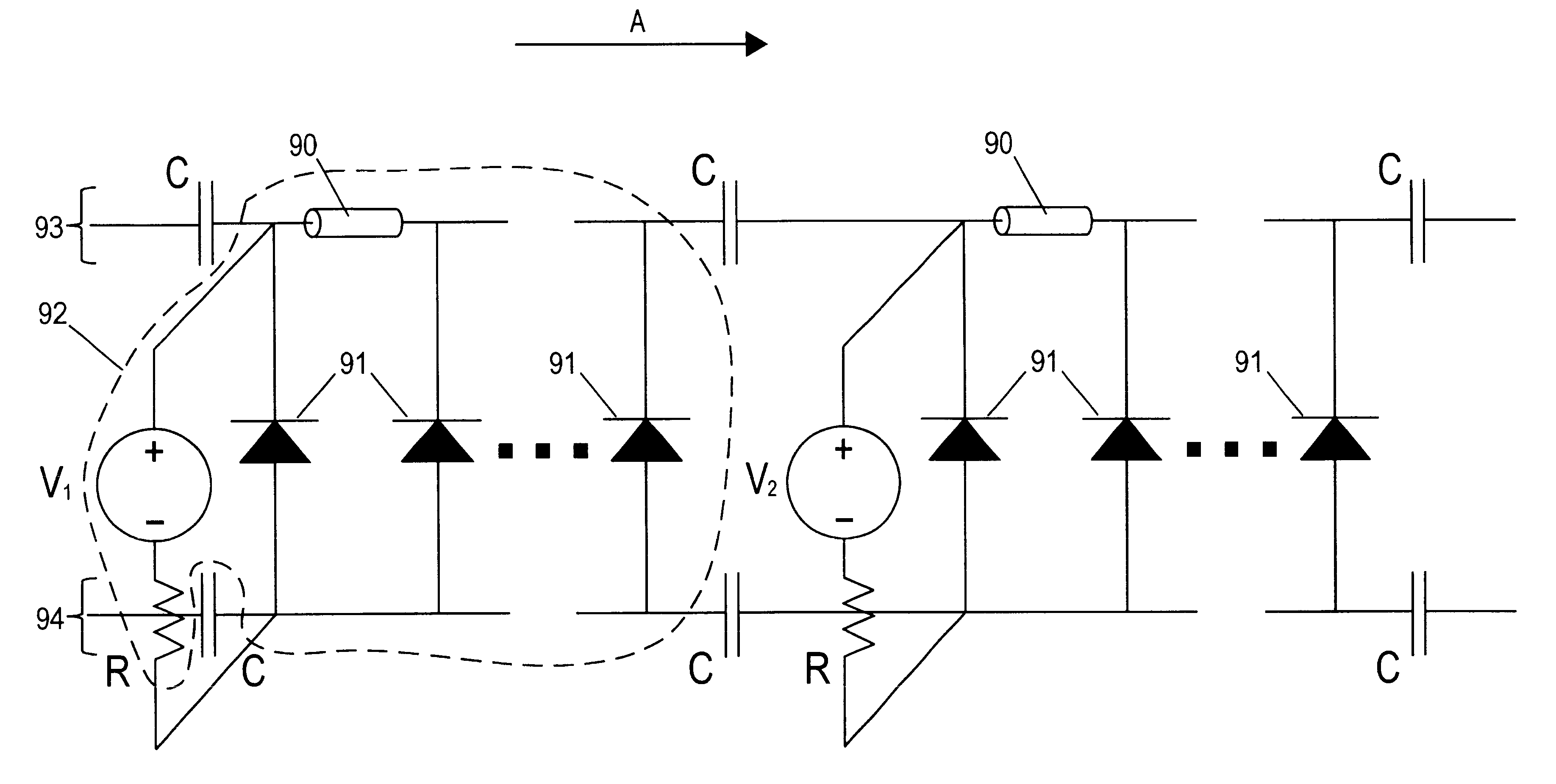
The term "non-linear transmission line (NLTL)" is used herein to refer to one or more transmission line sections augmented by reverse biased diodes. The transmission line sections and reverse biased diodes may be provided by a distributed diode which as such is a particular embodiment of an NLTL. Embodiments where the diodes are discrete are referred to herein as lumped NLTLs.

Prior art diodes are known which are made up of appropriately doped semiconductor forming a positive-negative (pn)-junction arranged such that current may flow through the junction. These are essentially two-terminal devices with one terminal connected to the positive (p) side and the other to the negative (n) side of the junction. The flow of cur...


PUM


Abstract

The principal reason that commercially available 10 gigabits per second electrical interconnect has not previously been available is that such interconnect structures possess too high a level of parasitic inductance, capacitance, resistance and conductance. These result in signal degradation as a result of attenuation, harmonic distortion and dispersion and so sufficiently error-free transmission of data has been virtually impossible for high data rates such as those around 5 gigabits per second and above. By providing compensation mechanisms, signal integrity is improved thus enabling reliable data transmission at data rates of 5 gigabits per second, 10 gigabits per second and above. Non-linear transmission lines are used to form these compensation mechanisms. The non-linear transmission line may take the form of a distributed diode, for example, formed from a layer of N-doped silicon covered on its top surface by a layer of platinum and on its bottom surface by a layer of silicon dioxide. Advantageously, voltage biased sections of NLTL are used to perform compensation for different regions of a signal pulse according to the particular voltage biasing used. A plurality of such voltage biased sections of NLTL may be connected in series in order to obtain improved signal compensation.

Description

The present invention relates to voltage biased sections of non-linear transmission lines. The invention is particularly related to, but in no way limited to the use of such non-linear transmission lines in interconnect structures for example, on printed circuit boards, back planes, integrated circuits, and surface mount device (SMD) packages.BACKGROUND TO THE INVENTIONModern large-scale electronics such as telecommunication or computing systems are usually comprised of many interconnected shelves of processing, access and / or memory modules. The processing, access and memory functions are usually provided by modules that plug into a large printed circuit board (PCB) referred to as a backplane (BP) or midplane (MP) located behind the modules. Due to the huge quantities of data available for processing and storage there is a need for ever-increasing data rates on the modules and BPs. With the advent of synchronous optical networks (SONET), telecommunication and computer systems may be...

Claims


Application Information

Patent Timeline
IPC IPC(8): H03K5/12H03K5/01H05K1/02
CPCH03K5/12H05K1/0237
Inventor WILLIAMSON, JOHN
Owner RPX CLEARINGHOUSE
Why Eureka
Try Eureka