Low-voltage differential signal (LVDS) transmitter with high signal integrity

a low-voltage differential and transmitter technology, applied in logic circuit coupling/interface arrangement, baseband system details, pulse techniques, etc., can solve the problems of degrading signal integrity, reducing signal integrity, and reducing signal integrity of conventional modern low-voltage differential signaling

Active Publication Date: 2006-04-25
SEMICON COMPONENTS IND LLC
View PDF8 Cites 35 Cited by
  • Summary
  • Abstract
  • Description
  • Claims
  • Application Information

AI Technical Summary

Benefits of technology

[0014]The foregoing problems with the prior state of the art are overcome by the principles of the present invention, which relate to a differential signal output driver circuit that has a positive output terminal and a negative output terminal. A first switching field effect transistor is coupled between a first voltage source and one of the output terminals. A second switching transistor is coupled between the first voltage source and the other of the output terminals. Similarly, a third switching transistor is coupled between a second voltage source and the positive output terminal. A fourth switching transistor is coupled between the second voltage source and the negative output terminal. The positive and negative output terminals are coupled together via a resistor or a series of resistors.

Problems solved by technology

Nevertheless, even conventional modern low voltage differential signaling has some drawbacks as will now be described with respect to FIG. 10.
This overshoot and undershoot degrades signal integrity.
This further degrades signal integrity.

Method used


Image

  • Low-voltage differential signal (LVDS) transmitter with high signal integrity
  • Low-voltage differential signal (LVDS) transmitter with high signal integrity
  • Low-voltage differential signal (LVDS) transmitter with high signal integrity

Examples


Embodiment Construction

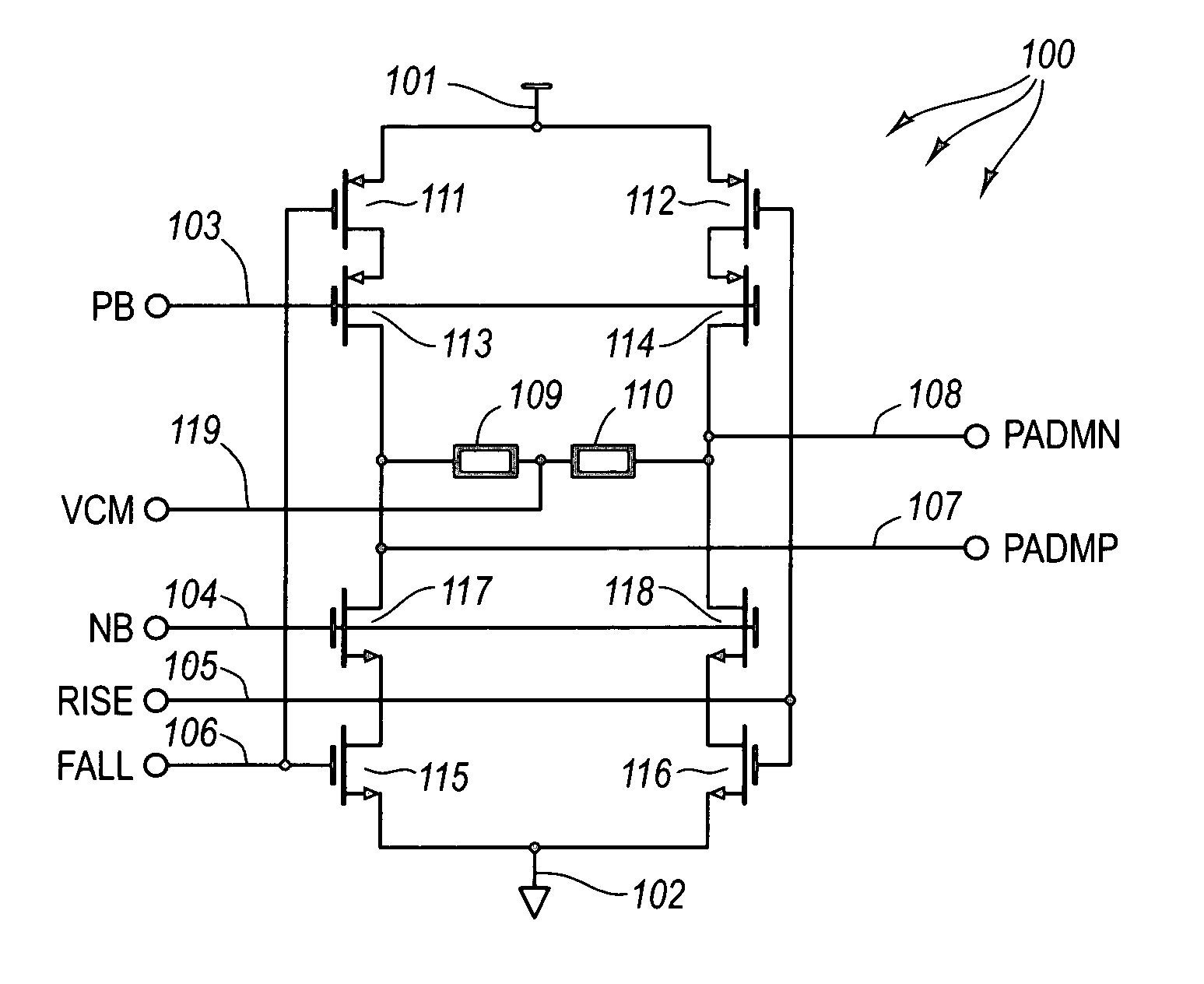
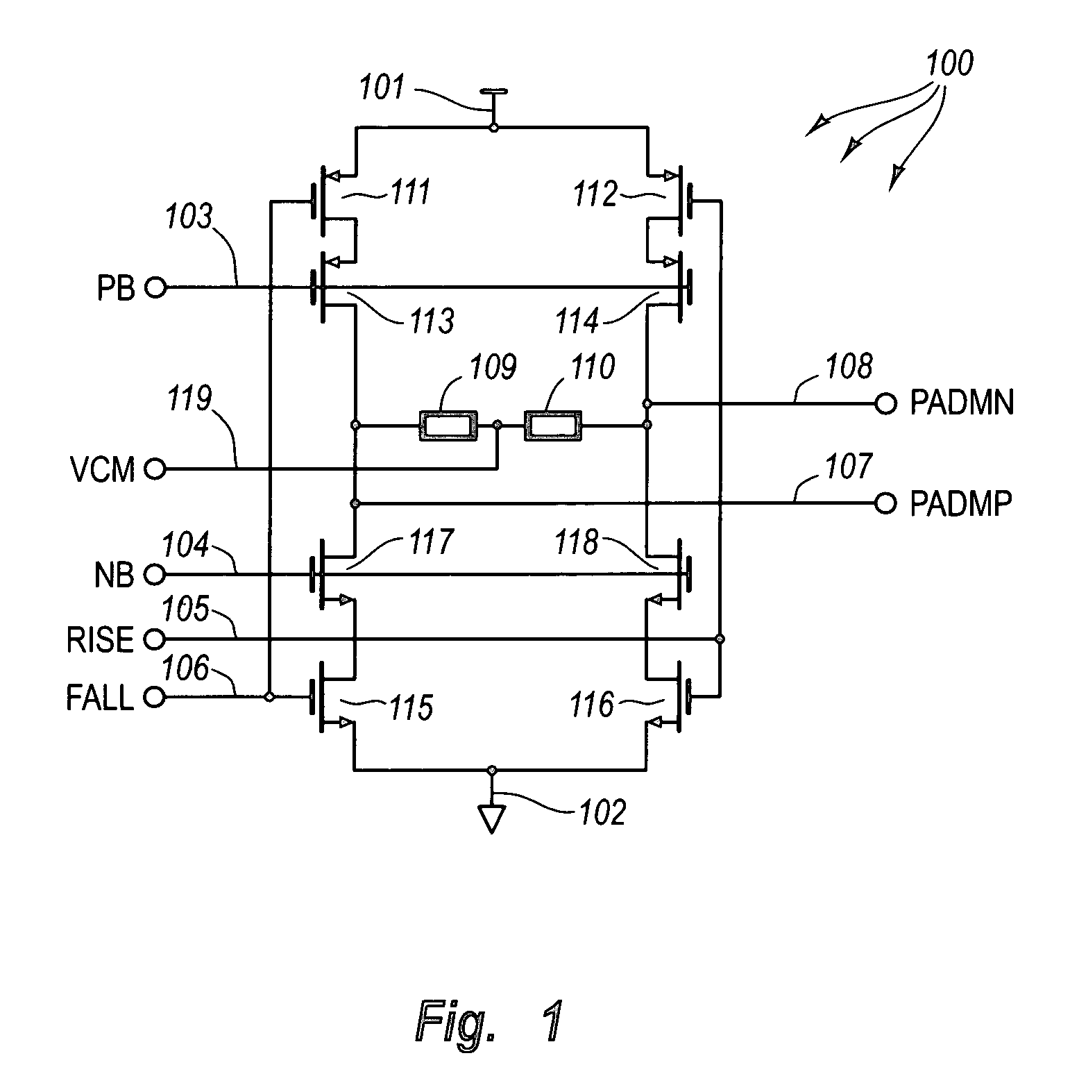
[0034]The principles of the present invention relate to a differential signal output driver circuit having four switching transistors. Bias transistors shield each of the switching transistors from the corresponding output terminal thereby blocking the Miller capacitance of the switching capacitor from generating overshoot or undershoot in the output differential voltage. Also, the output driver circuit may be driven by a differential skew cancellation circuit that generates a skew balanced differential signal to drive the switching transistors to further improve signal integrity. The signal path for generating each signal in the differential signal goes through a similar structure thereby ensuring similar propagation delay and thus small skew between the differential signals provided to the output driver circuit.

[0035]FIG. 1 is a circuit diagram of a low voltage differential signal output driver circuit 100 in accordance with one embodiment of the present invention in which bias tr...


PUM


Abstract

A differential signal output driver circuit having four switching transistors and having a bias transistor that shields each of the switching transistors from the corresponding output terminal thereby blocking the Miller capacitance of the switching capacitor from generating overshoot or undershoot in the output differential voltage. Also, the output driver circuit may be driven by a differential skew cancellation circuit that generates a balanced differential signal to drive the switching transistors to further improve signal integrity. The signal path for generating each signal in the differential signal goes through a similar structure thereby ensuring similar slew in each differential signal provided to the output driver circuit.

Description

BACKGROUND OF THE INVENTION[0001]1. The Field of the Invention[0002]The present invention relates generally to analog circuits. More specifically, the present invention relates to low-voltage differential signal transmitters that have high signal integrity.[0003]2. Background and Relevant Art[0004]Electronic circuitry provides complex functionality that is proving ever more useful. Electronic circuitry pervades our modern lives in areas such as communication, entertainment, travel, productivity, and the like. One useful circuit is the differential signal transmitter.[0005]Differential signaling offers several advantages over single-ended signaling. One is a significant reduction in Electro Magnetic Interference (EMI). Magnetic fields induced by one differential signal path tend to cancel out with magnetic fields induced by the other differential signal path. Differential signaling is also more resistant to negative effects of common mode noise. Differential signaling has been employ...

Claims


Application Information

Patent Timeline
Patent Type & Authority Patents(United States)
IPC IPC(8): H03K19/0175
CPCH04L25/028H04L25/0272
Inventor LI, ZHONGMIN
Owner SEMICON COMPONENTS IND LLC
Why Eureka
Try Eureka