Eureka AIR delivers breakthrough ideas for toughest innovation challenges, trusted by R&D personnel around the world.

Integrated circuit device, system, and method of fabrication

a technology of integrated circuits and fabrication methods, applied in the field of integrated circuits, can solve the problems of increasing the cost of lithography. and other fabrication processes and tools, and reducing or eliminating the effect of optical proximity correction

Inactive Publication Date: 2009-12-31
CARNEGIE MELLON UNIV
View PDF22 Cites 201 Cited by
  • Summary
  • Abstract
  • Description
  • Claims
  • Application Information

AI Technical Summary

Benefits of technology

[0009]It has been found that new methods, devices, and systems of fabrication are possible. These new methods, devices, and systems overcome many of the problems inherent in the prior art. For example, the present invention offers advantages over the prior art, such as compact size and the potential of repetitive pattern design.
[0024]In one embodiment, the present invention forms features in a regular, repeating pattern. These patterns may be formed, for example, with conventional fabrication techniques, such as by using a lithographic mask to form a pattern in a layer of photoresist and etching the exposed surface. The use of a regular, repeating pattern offers several advantages, including a relatively simple lithographic mask, the reduction or elimination of optical proximity correction (“OPC”) during fabrication, and increased throughput.

Problems solved by technology

In general, shorter wavelengths provide better resolution but are more expensive to implement and they create other problems.
Furthermore, physical limitations are presenting problems for the continued reduction in wavelengths in lithography.
Furthermore, the costs of lithography and other fabrication processes and tools have increased dramatically, and the research and development required for significant advances in various technologies will add to the costs.
There are also other problems with prior art integrated circuit technology.
For example, the design processes, the lithographic masks, and the lithographic processes involved in prior art integrated circuit design and fabrication are complex and expensive.
In addition, the utilization of integrated circuit area by active devices is relatively low.
As a result, prior art integrated circuit designs and processes are expensive and result in inefficient utilization of resources.
Those devices suffer a significant voltage drop between the controlling gate and the bulk semiconductor region as a result of charge in the charge storage gate that represents the memory value.
This problem is due to the stacking of a controlling gate and a charge storage gate in series with each other and above the bulk semiconductor region.
The ONO layer is difficult to fabricate because it is between two polysilicon layers that form the controlling and charge storage gates.
Finally, this structure of conventional flash memory devices also suffers from difficulties in the charging and discharging of the device.
In particular, the voltage drop from the controlling gate through the stored charge is significant and requires higher controlling gate voltages to affect the channel in the bulk semiconductor region.

Method used


Image

  • Integrated circuit device, system, and method of fabrication
  • Integrated circuit device, system, and method of fabrication
  • Integrated circuit device, system, and method of fabrication

Examples


second embodiment

[0095]The second embodiment is a complimentary VeSFET circuit using a TIG (“two independent gate”) configuration. In other words, each device includes two gates which are independently controlled. In the illustrated embodiment the right gate on each device is separately controlled (VPC and VNC) to provide for an “adjustable threshold voltage” (“ATV”) which can be independently controlled for each of the two devices. The adjustable threshold voltage may be static (“SATV”) or dynamic (“DATV”), and in some embodiments the adjustable threshold voltages may be the same for all transistors, or it may be different. The adjustable threshold voltages may be used, for example, to change the operational characteristics of the circuit. For example, at certain times the device may operate as a low-leakage device with a high threshold voltage, and at other time the device may operate as a high-speed device with a low threshold voltage. In some embodiments the device may operate in an intermediate...

third embodiment

[0098]The third embodiment is a complimentary VeSFET circuit using a SSSG (“source-shorted second gate”) configuration. In other words, the right side or “second gates” on each device are tied to the source of each device.

[0099]The fourth (far right) embodiment is a complimentary VeSFET circuit using a DSSG (“drain-shorted second gate”) configuration. In other words, the right side or “second” gates on each device are tied together and to the output. In this embodiment the output of the circuit also controls the signal on the right side or “second” gates.

fifth embodiment

[0100]The fifth embodiment is a complimentary VeSFET circuit using a FLSG (“floating second gate”) configuration. In other words, the right side or “second” gates are floating. In this embodiment, both devices are also PTV (“programmable threshold voltage”) devices and ATV (“adjustable threshold voltage”) devices. In other words, the second gates can be provided with a charge to program or adjust the threshold voltage of the particular device. The floating gates may be charged, for example, with an e-beam or with other means. In some embodiments the floating gates can be discharged, for example with the application of ultraviolet light, and then re-charged.

[0101]As used herein, PTV will refer to the process of programming a threshold voltage of a device to achieve a desired characteristic from the device. For example, one or more devices may be programmed to be in particular states, such as to route current in a particular path, to perform logic operations on signals, or to perform ...


PUM


Abstract

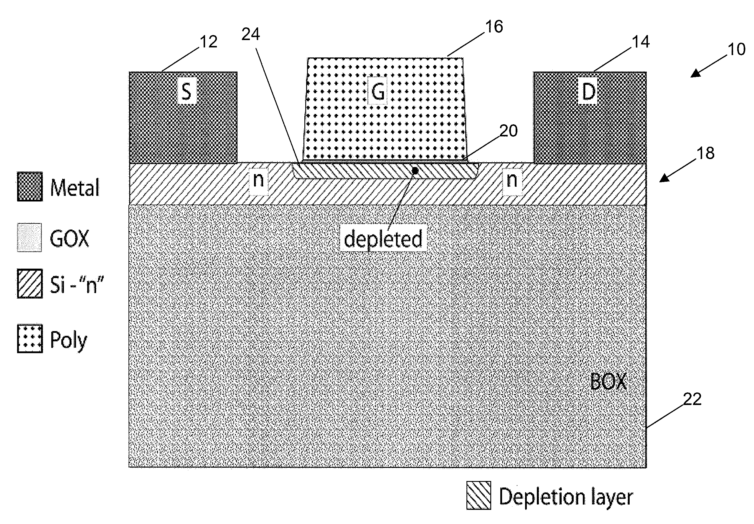
A semiconductor device, comprising a first semiconductor portion having a first end, a second end, and a slit portion, wherein the width of the slit portion is less than the width of at least one of the first end and the second end; a second portion that is a different material than the first semiconductor portion, a third portions that is a different material than the first semiconductor portion, wherein the second and third portions are on opposite sides of the slit portion, and at least three terminals selected from a group consisting of a first terminal connected to the first end, a second terminal connected to the second end, a third terminal connected to the second portion, and a fourth terminal connected to the third portion.

Description

FIELD OF THE INVENTION[0001]The present invention is directed generally to integrated circuits and, more specifically, to methods of fabricating integrated circuits, devices and systems for fabricating integrated circuits and other devices and systems, and devices and systems which are formed by, or which utilize, components or other parts which are formed by or in accordance with the present invention.BACKGROUND OF THE INVENTION[0002]The fabrication of integrated circuits is typically done by building successive layers on top of each other. These layers are built on or in an underlying substrate, such as single crystal silicon or an electrical insulator. When the substrate is an electrical insulator, such as sapphire, the fabrication techniques and resulting devices are often referred to as “silicon on insulator” or “semiconductor on insulator”, which are collectively called “SOI”.[0003]Many process steps are typically involved in semiconductor fabrication including deposition, oxi...

Claims


Application Information

Patent Timeline
IPC IPC(8): H01L29/786
CPCH01L27/1203H01L29/0692H01L29/66795H01L29/7881H01L29/7831H01L29/785H01L29/66825
Inventor MALY, WOJCIECH P.
Owner CARNEGIE MELLON UNIV
Why Eureka
Eureka Blog
Learn More