Film deposition device and substrate processing device

a technology of substrate and deposition device, which is applied in the direction of coating, chemical vapor deposition coating, metallic material coating process, etc., can solve the problems of large time loss, long processing time, and high time consumption of these operations, so as to reduce reactive gas consumption, improve wafer throughput, and increase the effect of throughpu

Inactive Publication Date: 2011-11-03
TOKYO ELECTRON LTD
View PDF3 Cites 360 Cited by
  • Summary
  • Abstract
  • Description
  • Claims
  • Application Information

AI Technical Summary

Benefits of technology

[0014]Most of source gases used for the ALD process are obtained by evaporating a liquid material or sublimating a solid material, and the source gases are expensive. Such expensive reactive gases are consumed in the amount more than the amount required for the film deposition, for the purpose of improvement in the throughput of the wafer. It is desirable to provide a film deposition device which is able to reduce the reactive gas consumption and increase the throughput.
[0015]In one aspect, the present disclosure provides a film deposition device and a substrate processing device which are capable of reducing the consumption of reactive gases and raising the throughput.Means For Solving The Problem

Problems solved by technology

In the case of the above film deposition method, much time is required for the gas replacement by the purge gas and the number of the gas supplying cycles amounts to hundreds of times. A long processing time is needed.
The time loss accompanying these operations is large.

Method used


Image

  • Film deposition device and substrate processing device
  • Film deposition device and substrate processing device
  • Film deposition device and substrate processing device

Examples


Embodiment Construction

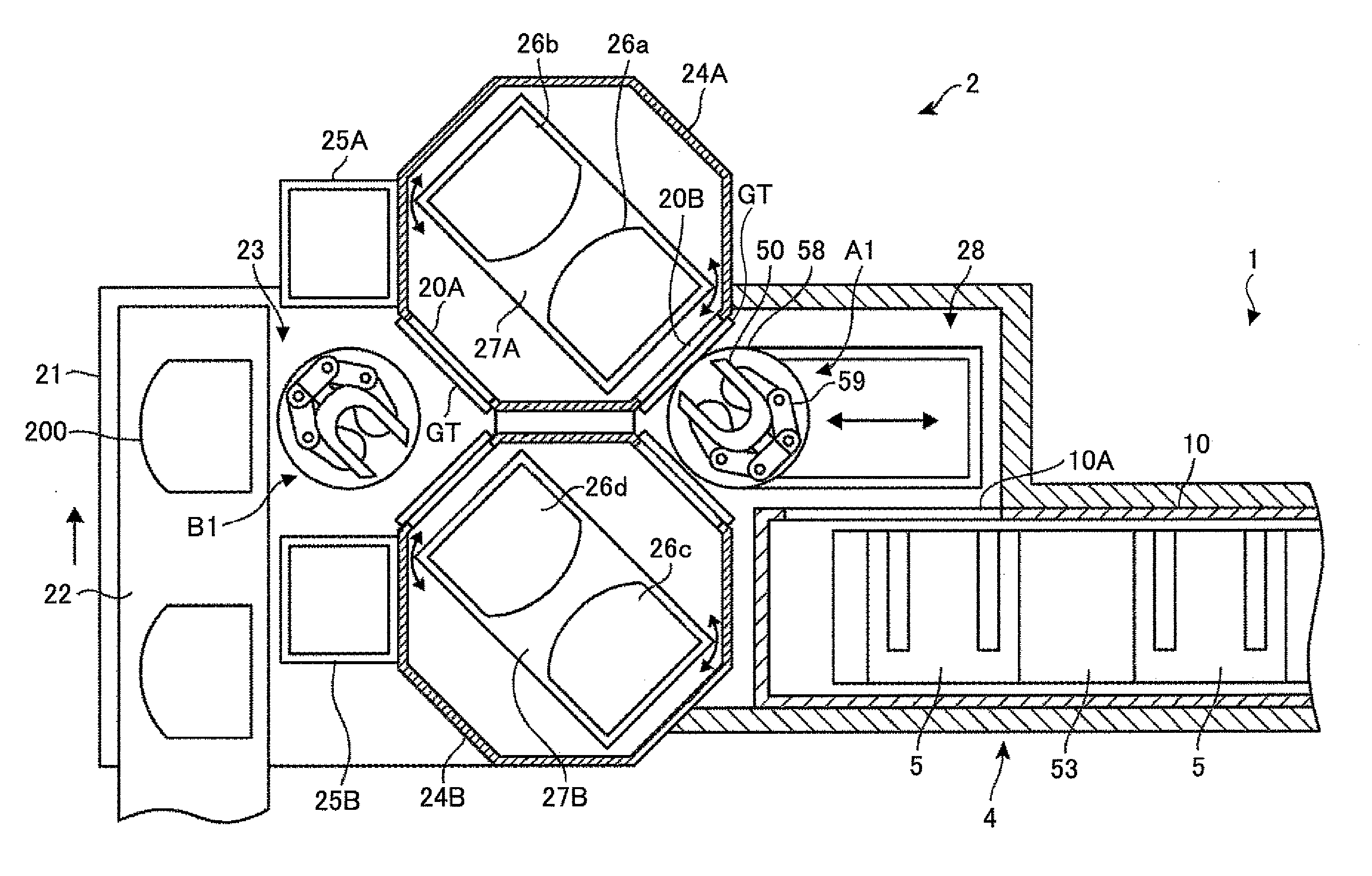
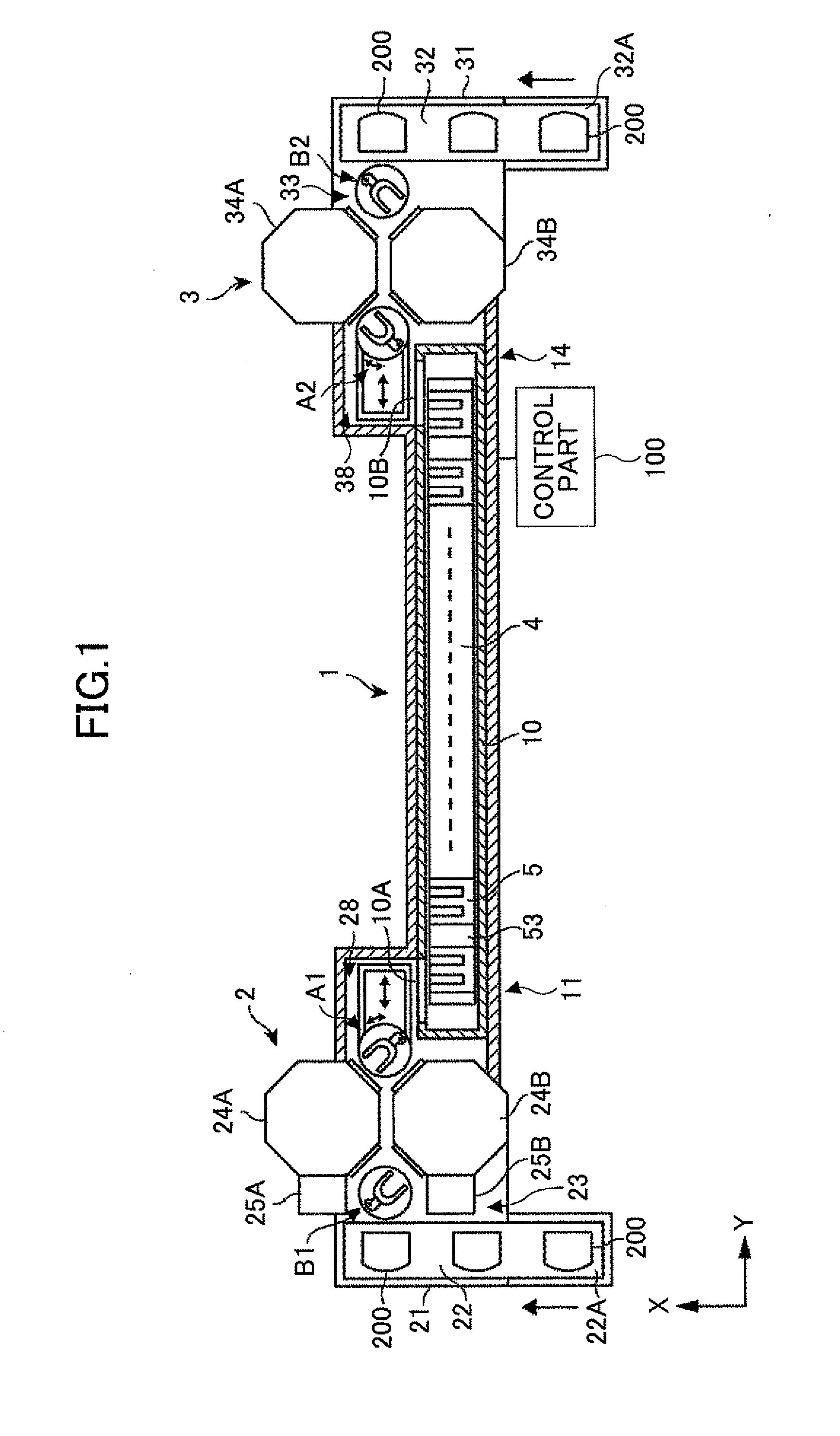
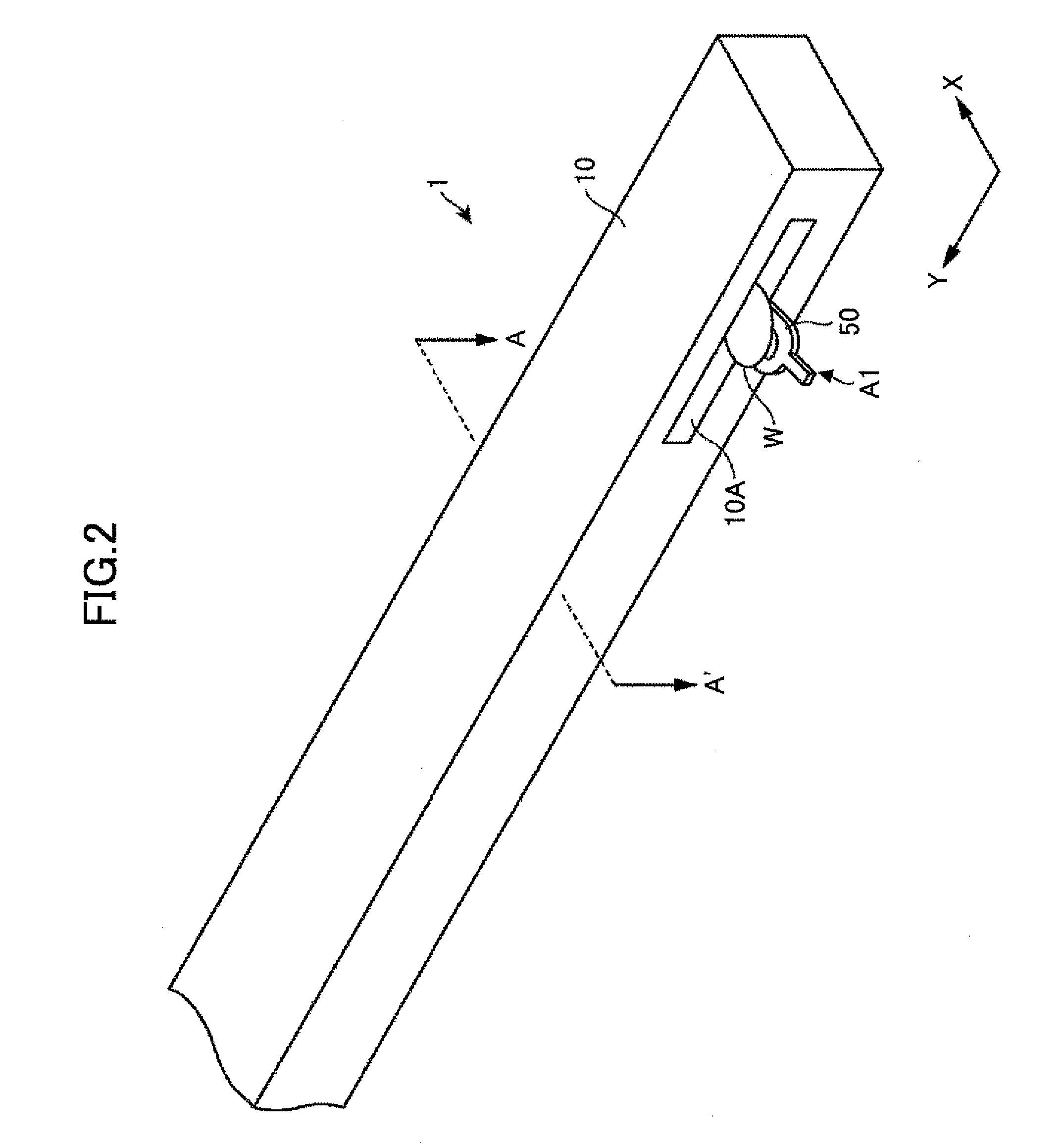
[0035]In a film deposition device of one embodiment of the present disclosure, a plurality of mutually reactive gases are sequentially supplied to a surface of a substrate and the gas supplying cycle is repeated a number of times, so that a plurality of resultant layers are laminated on the substrate surface to form a thin film thereon by the repeated gas supplying cycle. The substrate is transported in accordance with a circulatory transport path including a linear transport path, and a first reactive gas and a second reactive gas are sequentially supplied to the substrate to perform the gas supplying cycle, film deposition processing can be performed with high throughput. Moreover, a plurality of substrate mounting parts arranged in a row are transported in accordance with the circulatory transport path, and the moving speed at the time of transport is constant in the surface of the substrate. Hence, it is not necessary to supply a large amount of reactive gas to the region in whi...


PUM

PropertyMeasurementUnit
diameteraaaaaaaaaa
distanceaaaaaaaaaa
lengthaaaaaaaaaa

Abstract

A film deposition device includes a substrate transporting device arranged in a vacuum chamber to include a circulatory transport path in which substrate mounting parts arranged in a row are transported in a circulatory manner, the circulatory transport path including a linear transport path in which the substrate mounting parts are transported linearly. A first reactive gas supplying part is arranged along a transporting direction in which the substrate mounting parts are transported in the linear transport path, to supply a first reactive gas to the substrate mounting parts. A second reactive gas supplying part is arranged alternately with the first reactive gas supplying part along the transporting direction, to supply a second reactive gas to the substrate mounting parts. A separation gas supplying part is arranged to supply a separation gas to a space between the first reactive gas supplying part and the second reactive gas supplying part.

Description

TECHNICAL FIELD[0001]The present disclosure relates to a film deposition device and a substrate processing device in which at least two mutually reactive gases are sequentially supplied to a surface of a substrate and the gas supplying cycle is repeated a number of times, so that a plurality of resultant layers are laminated on the substrate surface to form a thin film thereon.BACKGROUND ART[0002]A film deposition process in a semiconductor fabrication process is known. In this process, a first reactive gas is supplied to a surface of a substrate, such as a semiconductor wafer W (wafer W), under a vacuum atmosphere. After the first reactive gas is adsorbed in the substrate surface, a second reactive gas is supplied to the substrate surface, and one or a plurality of atomic or molecular layers are formed by the reaction of these gases. By repeating the gas supplying cycle a number of times, these layers are laminated and a thin film is deposited on the substrate.[0003]This process is...

Claims


Application Information

Patent Timeline
Patent Type & Authority Applications(United States)
IPC IPC(8): C23C16/455C23C16/46C23C16/458
CPCC23C16/0245C23C16/45551C23C16/4583C23C16/54H01L21/67706H01L21/67173H01L21/67201H01L21/67346H01L21/67005
Inventor TSUJI, NORIHIKOMOROI, MASAYUKIYANAGITANI, KENICHIHANADA, YOSHIYUKI
Owner TOKYO ELECTRON LTD
Why Eureka
Try Eureka