Light-emitting diode device

A technology of light-emitting diodes and components, applied to electrical components, semiconductor devices, circuits, etc., can solve problems such as uneven luminous intensity, inability to solve current, and congestion, and achieve the effects of improving uniformity, solving current congestion, and improving uniformity

Inactive Publication Date: 2013-06-19
CHI MEI LIGHTING TECHNOLOGY CORP +1
View PDF3 Cites 13 Cited by
  • Summary
  • Abstract
  • Description
  • Claims
  • Application Information

AI Technical Summary

Problems solved by technology

[0005] However, according to the experimental results, only setting the current blocking structure 16 can only slightly improve the problem of uneven luminous intensity, but cannot solve the fundamental problem of current crowding, so the uniformity of luminous intensity cannot be greatly improved

Method used


Image

  • Light-emitting diode device
  • Light-emitting diode device
  • Light-emitting diode device

Examples


Embodiment Construction

[0046] A light emitting diode element according to a preferred embodiment of the present invention will be described below with reference to related drawings, wherein the same elements will be described with the same reference symbols.

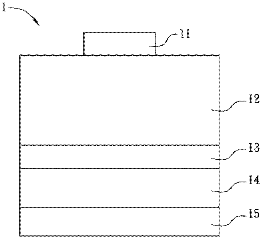
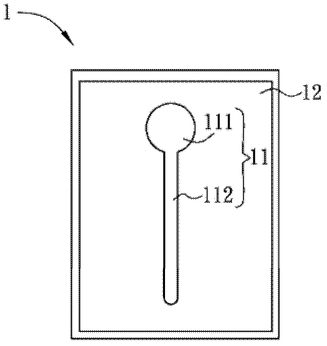
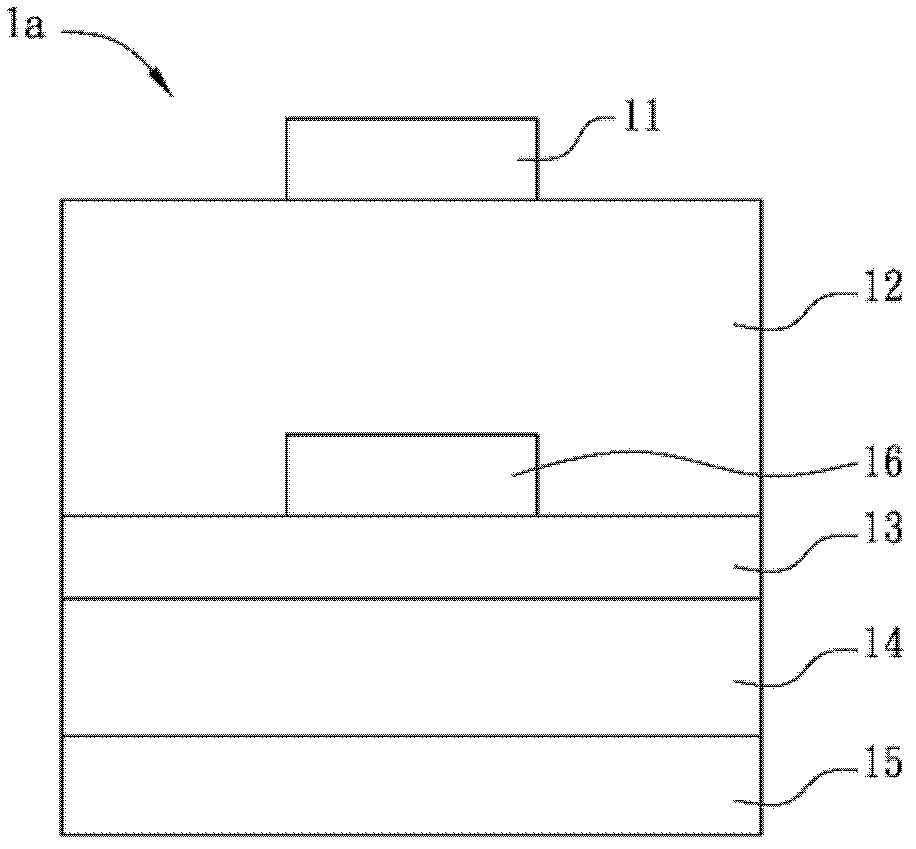
[0047] Figure 4 It is a schematic diagram of a light emitting diode element 2 in a preferred embodiment of the present invention. The LED device 2 includes a substrate 21 , an epitaxial layer 22 , a first electrode 23 , a second electrode 24 , a connection layer 25 and a light-transmitting conductive layer 27 .

[0048] The substrate 21 is a conductive substrate, which includes a conductive material, and the conductive substrate can be selected to facilitate heat dissipation. The substrate 21 may include a conductive material or a mixture of conductive and non-conductive materials; the conductive material is, for example, silicon carbide (SiC) or silicon or copper. The substrate 21 is, for example, a silicon carbide (SiC) substrate, a silic...


PUM


Abstract

A light-emitting diode device includes a substrate, an epitaxial layer and a first electrode. The epitaxial layer is disposed on the substrate. The first electrode is disposed on the epitaxial layer and includes a connecting portion and a conductive finger. The conductive finger has a first end and a second end, and the first end is connected to the connecting portion. At least one portion of the conductive finger is tapered along an extending direction of the conductive finger.

Description

technical field [0001] The invention relates to a light emitting diode element. Background technique [0002] A light-emitting diode (LED) is a light-emitting element made of semiconductor materials. Since light-emitting diodes belong to cold light, they have the advantages of low power consumption, long life of components, fast response speed, etc., coupled with the characteristics of small size and easy to make extremely small or array components, so in recent years, with the continuous advancement of technology, Its application scope covers indicator lights of computers or home appliances, backlights of liquid crystal display devices, traffic signs or vehicle lights. [0003] figure 1 Shown is a conventional light emitting diode device 1 , which includes a first electrode 11 , an epitaxial layer 12 , a connection layer 13 , a conductive substrate 14 and a second electrode 15 , and the above devices are stacked in sequence. figure 2 It is a schematic top view of the LE...

Claims


Application Information

Patent Timeline
Patent Type & Authority Applications(China)
IPC IPC(8): H01L33/38H01L33/14
CPCH01L33/145H01L33/38
Inventor 林忠欣邱信嘉吴奇隆张瑞君朱长信
Owner CHI MEI LIGHTING TECHNOLOGY CORP
Why Eureka
Try Eureka