
Improved LED welding technique

A welding process and welding point technology, applied in the field of improved LED welding process, can solve the problems such as the influence, inconvenience and offset of the effective light utilization rate of the LED backlight module 1', and achieve the effect of improving the effective light utilization rate.

Inactive Publication Date: 2013-07-03
苏州世鼎电子有限公司
View PDF6 Cites 2 Cited by
  • Summary
  • Abstract
  • Description
  • Claims
  • Application Information

AI Technical Summary

Problems solved by technology

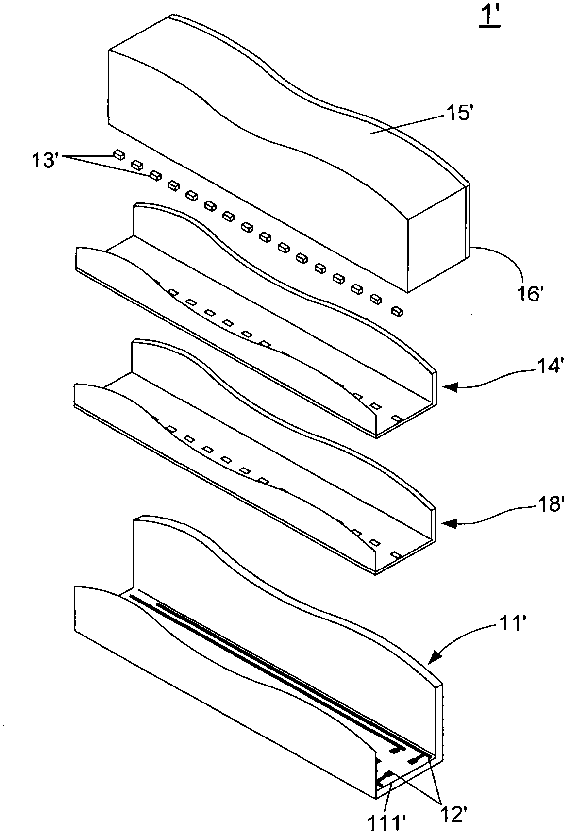
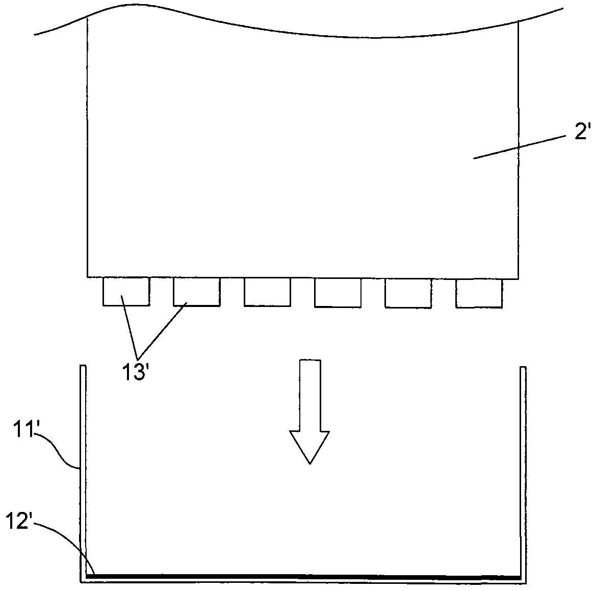
[0008] 3. Based on the first point above, in addition, during the reflow process, since the LED element 13' is only placed on the copper circuit layer 12' and is not restricted, once the LED element 13' is slightly vibration, some LED elements 13' will be shifted, and these shifted LED elements 13' will also have a considerable impact on the effective light utilization rate of the LED backlight module 1'
[0009] This shows that the above-mentioned existing LED welding process obviously still has inconvenience and defects in the manufacturing method and use, and needs to be further improved urgently.
In order to solve the above-mentioned problems, the relevant manufacturers have tried their best to find a solution, but no suitable design has been developed for a long time, and the general manufacturing method has no suitable manufacturing method to solve the above-mentioned problems. Obviously, It is a problem that relevant industry players are eager to solve

Method used


Image

  • Improved LED welding technique
  • Improved LED welding technique
  • Improved LED welding technique

Examples


no. 3 example

[0125] In addition, the improved LED soldering method of the present invention has a third embodiment, please refer to Figure 15A and Figure 15B , is a method flow chart of the third embodiment of an improved LED welding process method of the present invention; as Figure 15A and Figure 15B As shown, the third embodiment of the improved LED welding process method of the present invention includes the following steps:

[0126] Firstly, execute the step (S01"), arranging a first insulating and thermally conductive adhesive 18a on a cover bottom 111 of a cover 11; then, execute the step (S02"), a copper foil circuit layer 12 is arranged on a first On the second insulating and heat-conducting adhesive 18; then, perform step (S03"), attach the second insulating and heat-conducting adhesive 18 provided with the copper foil circuit layer 12 to the cover bottom provided with the first insulating and heat-conducting adhesive 18a 111. Continuing, then execute the step (S04"), usin...


PUM


Abstract

The invention provides an improved LED welding technique. The method comprises that the use of a spacing belt and a down pressing jig is added during the welding process of an LED element, so that, when the welding technology to the LED element is finished, each LED element welded on a copper circuit layer is enabled to be have the same height, therefore, the efficient light utilization efficiency of an LED backlight module is increased; according to the method, during the welding process of the LED element, the first insulating and heat conducting glue is attached to the bottom of a cover body, a second insulating and heat conducting glue arranged on the copper foil circuit layer is attached to the first insulating and heat conducting glue, in this way, a copper foil circuit layer is arranged at the bottom of the cover body, and the phenomenon of glue overflow can be avoided; besides, the spacing belt has the function of limiting the moving of the LED element. Therefore, when welding technology is performed on the LED element, the problem of shifting of the LED element is not required to be worried.

Description

technical field [0001] The invention relates to a welding process method, in particular to an improved LED welding process method designed for LED backlight modules and LED lamps. Background technique [0002] Light-emitting diodes (Light-Emitting Diodes, LEDs) are currently widely used light-emitting elements, and are widely used in daily life of human beings due to their advantages of small size and long service life. [0003] Light-emitting diodes (LEDs) are most commonly used as lighting devices, and, in addition to being used in lighting devices, light-emitting diodes are more widely used in backlight modules, see figure 1 , is a three-dimensional view of a commonly used LED backlight module, such as figure 1 As shown, the LED backlight module 1' includes: a cover body 11', a copper circuit layer 12', a plurality of LED elements 13', a heat conduction layer 18', a reflector 14', a light guide plate 15' and a Bottom reflector 16'. Wherein the cover 11' has a cover bot...

Claims


Application Information

Patent Timeline
Patent Type & Authority Applications(China)
IPC IPC(8): B23K1/00B23K1/20
Inventor 陈灿荣
Owner 苏州世鼎电子有限公司
Learn More