Thin-film photovoltaic cell and manufacturing method thereof
A technology of thin-film photovoltaic cells and manufacturing methods, which can be used in photovoltaic power generation, final product manufacturing, sustainable manufacturing/processing, etc., and can solve problems such as low effective light utilization rate and thick absorbing layer
- Summary
- Abstract
- Description
- Claims
- Application Information
AI Technical Summary
Problems solved by technology
Method used
Image
Examples
Embodiment Construction
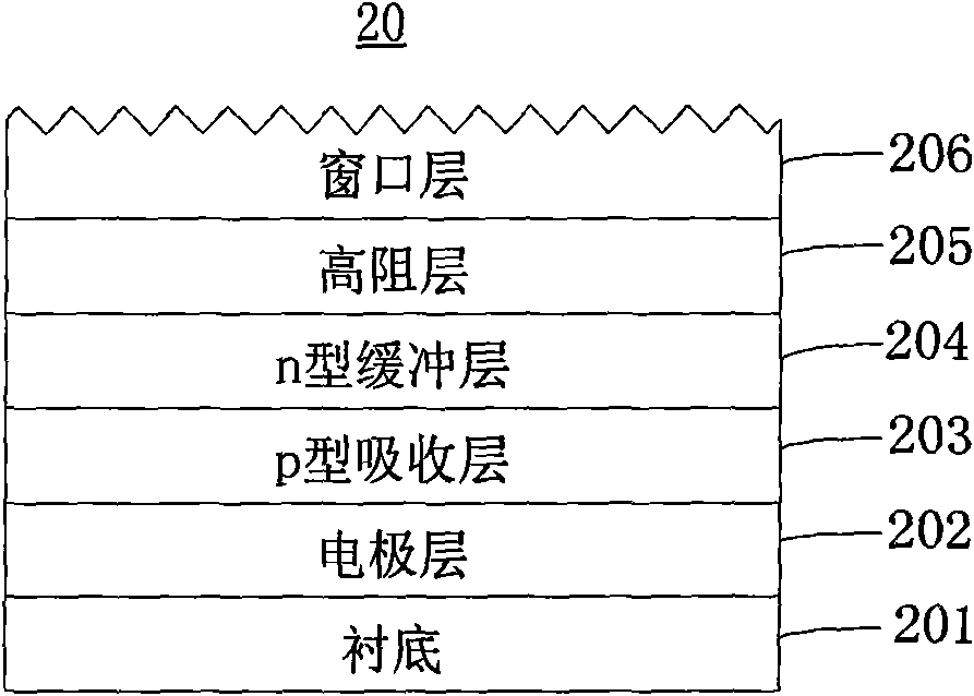
[0025] figure 1 is a schematic diagram of the first embodiment of a CIGS / CIS thin film photovoltaic cell. From bottom to top are substrate 201 , electrode layer 202 , p-type absorber layer 203 , n-type buffer layer 204 , high resistance layer 205 and window layer 206 . The substrate 201 can be a soda-lime glass substrate, the electrode layer 202 can be a molybdenum electrode layer, the material of the p-type absorption layer 203 is CIGS / CIS, the material of the n-type buffer layer 204 is CdS, and the material of the high resistance layer 205 is ZnO , the window layer 206 is a ZnO-based transparent conductive window layer with low absorption and high conductance in the near-infrared band, and the window layer 206 adopts a light-trapping structure.
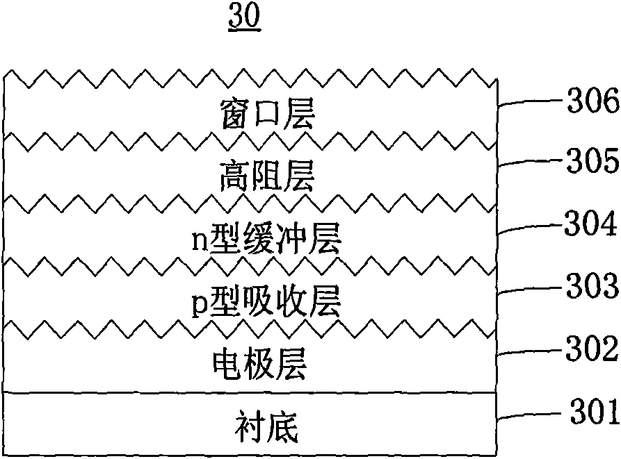
[0026] The light-trapping structure refers to the uneven shape of the surface. Specifically, it can be in the shape of ripples, V-shaped grooves, random or uniformly distributed pyramid shapes, and the like. The light-trapping st...
PUM
 Abstract
Description
Claims
Application Information


