Thin-film photovoltaic cell and manufacturing method thereof

A thin-film photovoltaic cell and manufacturing method technology, applied in photovoltaic power generation, final product manufacturing, sustainable manufacturing/processing, etc., can solve problems such as low effective light utilization rate, thick absorption layer, etc.

Active Publication Date: 2011-01-12
珠海中科先进技术研究院有限公司
View PDF0 Cites 12 Cited by
  • Summary
  • Abstract
  • Description
  • Claims
  • Application Information

AI Technical Summary

Problems solved by technology

[0005] In view of this, it is necessary to provide a thin-film photovoltaic cell that can greatly reduce the thickness of the absorbing layer of the battery, save raw materials, and significantly

Method used


Image

  • Thin-film photovoltaic cell and manufacturing method thereof
  • Thin-film photovoltaic cell and manufacturing method thereof
  • Thin-film photovoltaic cell and manufacturing method thereof

Examples


Embodiment Construction

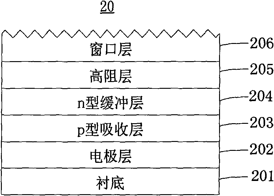
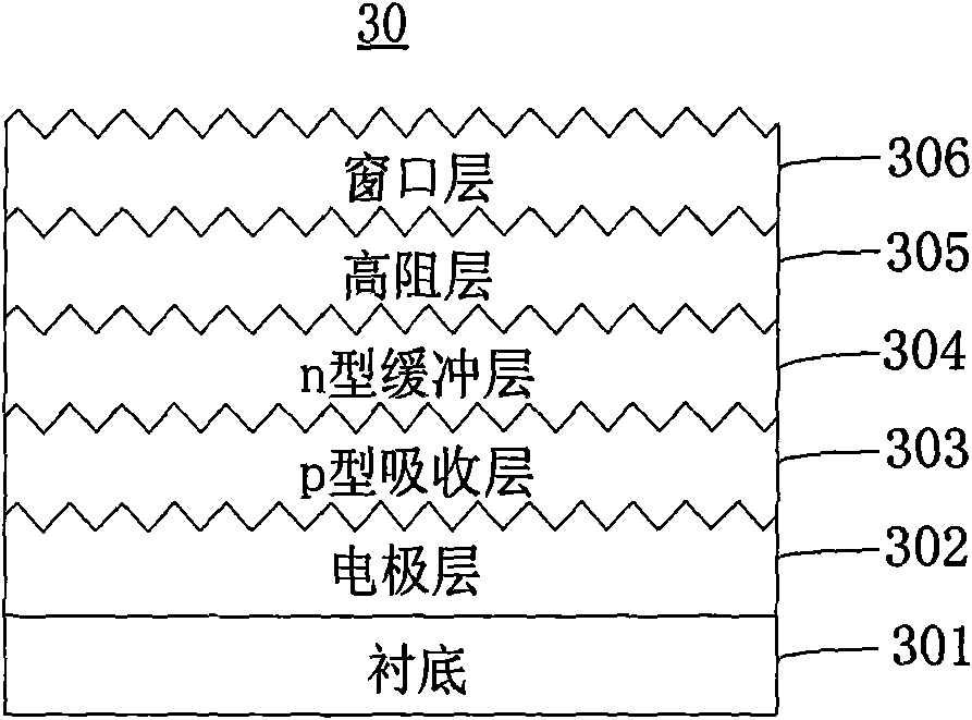
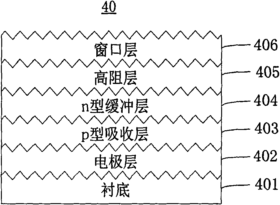
[0025] figure 1 is a schematic diagram of the first embodiment of a CIGS / CIS thin film photovoltaic cell. From bottom to top are substrate 201 , electrode layer 202 , p-type absorber layer 203 , n-type buffer layer 204 , high resistance layer 205 and window layer 206 . The substrate 201 can be a soda-lime glass substrate, the electrode layer 202 can be a molybdenum electrode layer, the material of the p-type absorption layer 203 is CIGS / CIS, the material of the n-type buffer layer 204 is CdS, and the material of the high resistance layer 205 is ZnO , the window layer 206 is a ZnO-based transparent conductive window layer with low absorption and high conductance in the near-infrared band, and the window layer 206 adopts a light-trapping structure.

[0026] The light-trapping structure refers to the uneven shape of the surface. Specifically, it can be in the shape of ripples, V-shaped grooves, random or uniformly distributed pyramid shapes, and the like. The light-trapping st...


PUM

PropertyMeasurementUnit
Thicknessaaaaaaaaaa
Thicknessaaaaaaaaaa

Abstract

The invention relates to a thin-film photovoltaic cell and a manufacturing method thereof. The thin-film photovoltaic cell comprises a lining, an electrode layer, a p-type absorption layer, an n-type buffer layer, a high-resistance layer and a window layer, which are sequentially arranged in an overlapping way from the bottom up. The window layer is a near infrared waveband low-absorption high-conductivity ZnO-based transparent conductive window layer. The thin-film photovoltaic cell is in a light trapping structure. The manufacturing method of the thin-film photovoltaic cell comprises the steps of: providing a lining; depositing an electrode layer; depositing a p-type absorption layer; depositing an n-type buffer layer; depositing a high-resistance layer; depositing a near infrared low-absorption ZnO-based window layer; and forming a light trapping structure. The thin-film photovoltaic cell has the absorption layer of small thickness and has higher effective light utilization ratio.

Description

technical field [0001] The invention relates to a thin film photovoltaic cell and a manufacturing method thereof. Background technique [0002] Copper indium gallium selenide / copper indium selenide (CIGS / CIS) thin-film photovoltaic cells have the advantages of low cost, high efficiency, and good stability, and are recognized as the second-generation photovoltaic cells with the most development and market potential. People's research on it began in the early 1980s. After more than 20 years of development, the theoretical research and preparation process of CIGS / CIS thin-film photovoltaic cells have achieved gratifying results. At present, its highest laboratory photoelectric conversion efficiency reaches 19.9%. (NREL), which is currently the thin-film photovoltaic cell with the highest conversion efficiency. [0003] The upper limit of the long-wave absorption wavelength of the traditional CIGS / CIS thin-film photovoltaic cell absorbing layer can reach 1100nm, and the light a...

Claims


Application Information

Patent Timeline
IPC IPC(8): H01L31/042H01L31/0236H01L31/18H01L31/0445H01L31/0749
CPCY02E10/50Y02E10/541Y02P70/50
Inventor 宋秋明肖旭东强骥鹏施成营刘壮陈旺寿
Owner 珠海中科先进技术研究院有限公司
Why Eureka
Try Eureka