
Active array display, scanning line drive circuit of active array display and scanning line drive method of active array display

An active array and driving method technology, applied in static indicators, instruments, etc., can solve the problems of precise resistance matching, horizontal stripes, and elimination, and achieve a uniform display effect

Active Publication Date: 2013-07-03
SHANGHAI TIANMA MICRO ELECTRONICS CO LTD
View PDF9 Cites 7 Cited by
  • Summary
  • Abstract
  • Description
  • Claims
  • Application Information

AI Technical Summary

Problems solved by technology

However, due to the limitations of technology and materials, it is very difficult to precisely match the resistance of the scanning leads of each scanning line, and it is difficult to eliminate the horizontal stripes well.

Method used


Image

  • Active array display, scanning line drive circuit of active array display and scanning line drive method of active array display
  • Active array display, scanning line drive circuit of active array display and scanning line drive method of active array display
  • Active array display, scanning line drive circuit of active array display and scanning line drive method of active array display

Examples


Embodiment 1

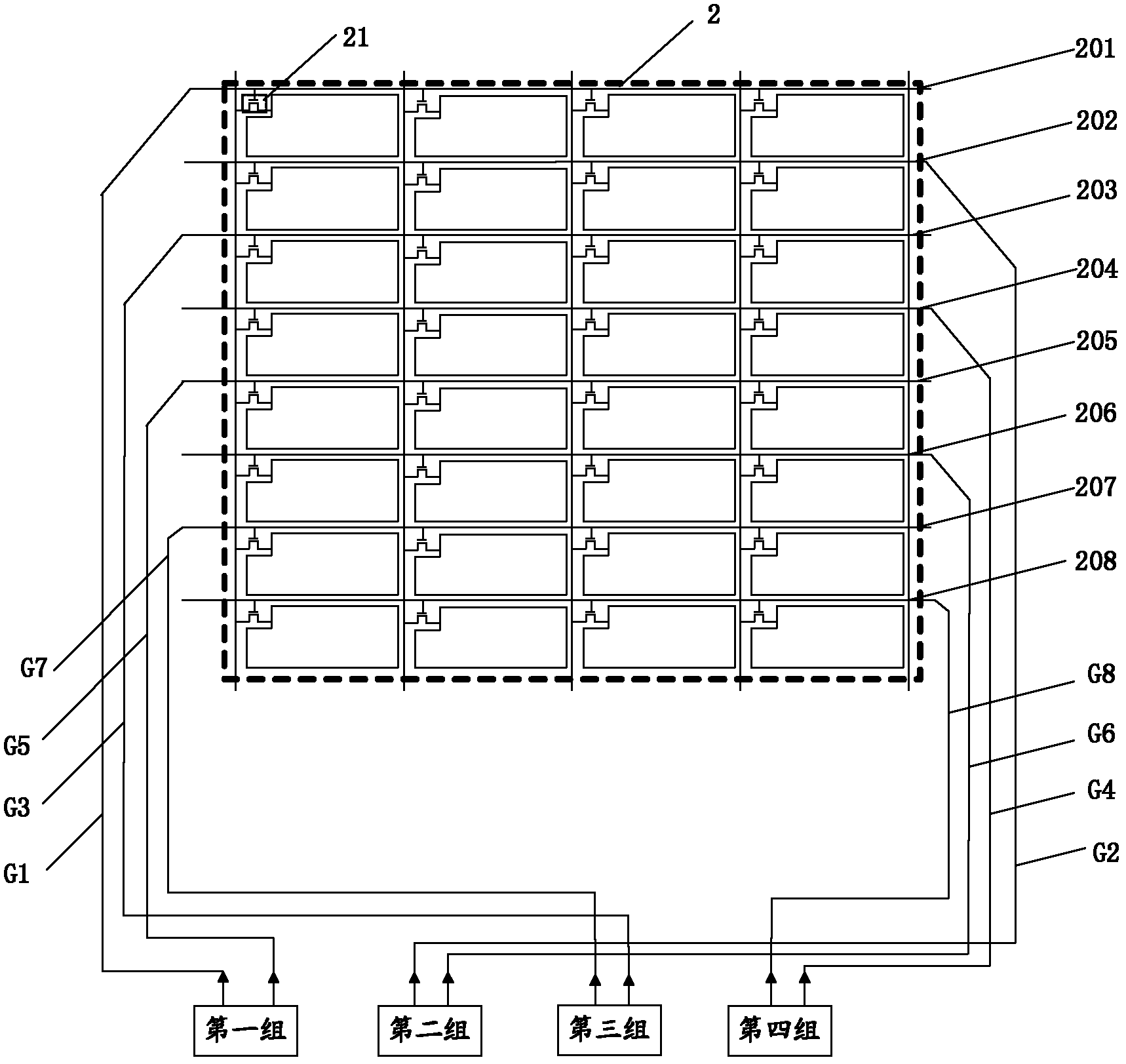
[0066] In the first embodiment, for the sake of brevity, the display area formed by 8 rows of pixels is taken as an example.

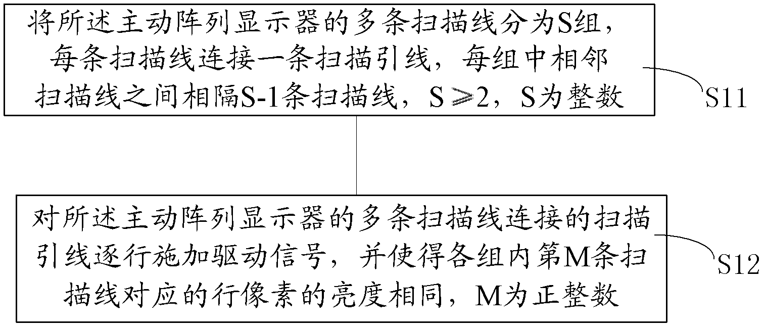
[0067] refer to figure 1 As shown, the scanning line driving method of the liquid crystal display provided in the first embodiment will be described in detail below.

[0068] First execute S11, divide the 8 scanning lines of the liquid crystal display into 4 groups, each scanning line is connected to a scanning lead, and the adjacent scanning lines in each group are separated by 3 scanning lines. The adjacency here does not refer to the actual adjacency of the scanning lines, but the adjacency of the scanning lines in each group from large to small or from small to large according to their actual order.

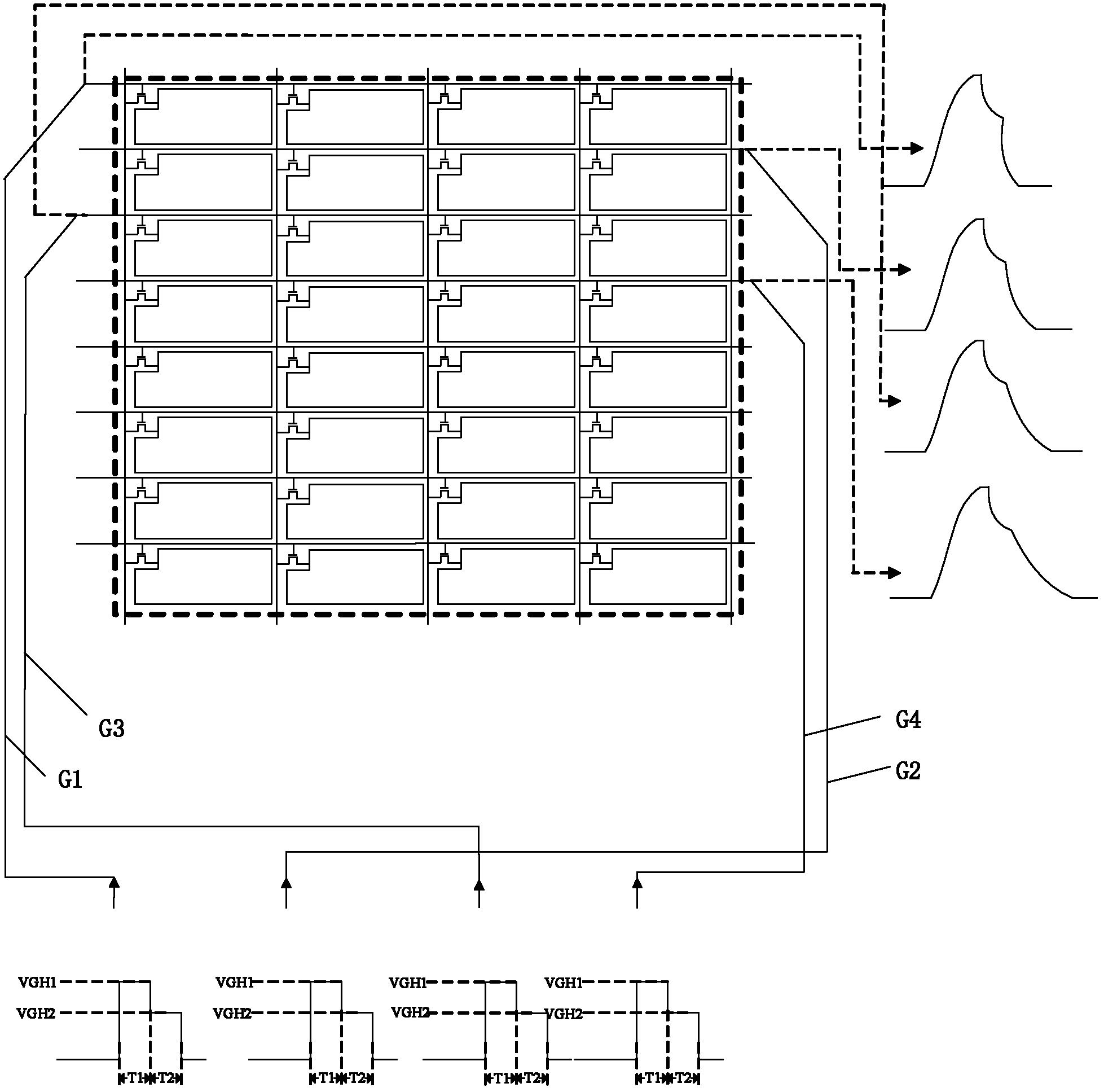
[0069] refer to figure 2 As shown, the liquid crystal display includes a display area 2 inside the dotted line frame and a non-display area outside the dotted line frame. In the display area 20, eight scan lines 201-208 are horizontally arranged, a...

Embodiment 2

[0116] What is described in Embodiment 1 is the case where the scanning lines 201-208 of the display are divisible. More generally, the existing liquid crystal display has 1024×768 pixels and 1024 row scanning lines. If it is divided into 10 groups, there will be different divisible case.

[0117] In view of the above situation, the figure 2 The display area is composed of 8 rows of pixels shown as an example, each row of pixels corresponds to 1 scan line, and the display is from top to bottom, respectively the first row 201 , the second row 202 , ... the eighth row 208 .

[0118] First execute S11', divide the 8 scanning lines 201-208 of the liquid crystal display into 3 groups, and the adjacent scanning lines in each group are separated by 2 scanning lines. The adjacency here still follows the explanation of the first embodiment.

[0119] After this step is performed, if Figure 13 As shown, the eight scanning lines 201-208 are divided into three groups, the first group:...


PUM


Abstract

The invention provides a scanning line drive method of an active array display. The method includes: dividing a plurality of scanning lines of the active array display into S groups, connecting each scanning line with one scanning lead, arranging S-1 scanning lines between two adjacent scanning lines in each group, S>=2 and is an integer; exerting drive signals on the scanning leads which are connected with the plurality of scanning lines of the active array display line by line, and enabling luminance of line pixels to match with each other, and the luminance of the line pixels corresponds to the Mth scanning lines in all the groups. In addition, the invention further provides a drive circuit of the scanning lines of the active array display and an active array display with the drive circuit. Due to the adoption of the technical scheme, the problem that display effects of scanning lines of an existing active array display are not the same is solved.

Description

technical field [0001] The invention relates to the display field, in particular to an active array display, a scanning line driving method of the active array display, and a scanning line driving circuit of the active array display. Background technique [0002] The existing active matrix display includes a pixel array, a plurality of scan lines connected to the pixel array and a plurality of data lines connected to the pixel array, each pixel includes a pixel electrode and a thin film transistor TFT, and the pixel electrode is connected to the pixel electrode through the thin film transistor TFT. Corresponding scan lines are coupled to data lines (ie, the pixel electrodes are electrically connected to the drain of the TFT, the scan lines are electrically connected to the gate of the TFT, and the data lines are electrically connected to the source of the TFT). During the display process, the scanning line driving circuit (usually an integrated circuit IC) of the active arra...

Claims


Application Information

Patent Timeline
IPC IPC(8): G09G3/20G09G3/36
Inventor 任虎男
Owner SHANGHAI TIANMA MICRO ELECTRONICS CO LTD
Learn More