
A test method for measuring the interface strength of copper filled tsv holes

A technology of interface strength and testing method, applied in the direction of measuring devices, mechanical devices, instruments, etc., can solve the problem that the TSV-Cu structure is not easy to experiment, and achieve the effect of accurate strength, reliable results, and guaranteed accuracy

Inactive Publication Date: 2015-08-12
BEIJING UNIV OF TECH
View PDF7 Cites 0 Cited by
  • Summary
  • Abstract
  • Description
  • Claims
  • Application Information

AI Technical Summary

Problems solved by technology

[0005] The present invention proposes a test method for measuring the interface strength of TSV-Cu after electroplating copper, including an experimental method and a data processing method. The experimental method solves the problem that the micron-scale TSV-Cu structure is not easy to carry out experiments; the data processing method is aimed at The structural characteristics of TSV and the special material properties of copper-silicon can accurately separate the different work done by the indenter, and finally obtain the interface cracking work done by the indenter, and then obtain the critical strain energy release rate of the interface

Method used


Image

  • A test method for measuring the interface strength of copper filled tsv holes
  • A test method for measuring the interface strength of copper filled tsv holes
  • A test method for measuring the interface strength of copper filled tsv holes

Examples


Embodiment Construction

[0032] The present invention is described in detail below in conjunction with accompanying drawing:

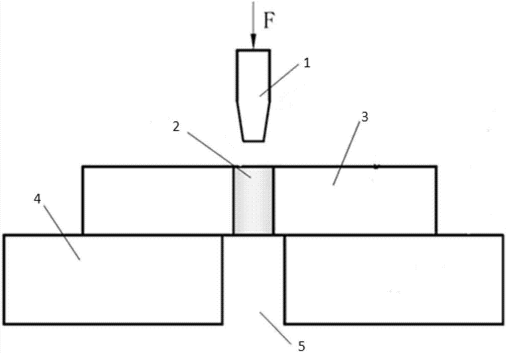
[0033] figure 1 It is a schematic diagram of the experimental principle. During the experiment, the sample carrier 4 is placed on the displacement stage of the nanoindenter, and the electroplated copper column 2 is aligned with the indenter 1 of the nanoindenter, and the electroplated copper column 2 is aligned with the carrier platform. Center the through hole 5, apply the force in the direction shown in the figure to press the electroplated copper column 2 out of the TSV through hole, and record the change of load and displacement during extrusion, and obtain the curve of load displacement. In the figure, the top of the electroplated copper column 2, that is, the end in contact with the indenter is the loading end of the electroplated copper column 2, and the bottom end of the electroplated copper column is the supporting end of the electroplated copper column 2.

[0034] S...


PUM


Abstract

The invention discloses a testing method for measuring interfacial strength of a copper filling TSV (Through Silicon Via), and belongs to the field of three-dimensional electronic packaging testing. The method comprises the steps that a TSV electrocoppering pillar is extruded from a TSV through hole by a nanoindentor to obtain load on a pressure head / a displacement curve in the extrusion process; unloading and reloading are carried out in different stages of extrusion to obtain an unloading curve and a loading curve; and the distance between a copper pillar top end after unloading to the upper surface of a TSV adapter board is obtained by using an atomic force microscope (AMF). The energy consumed by interface destroy, namely interface cracking power can be obtained through analysis, and a critical strain energy release rate of an interface can be obtained through dividing an area of the destroyed interface with the interface cracking power. With the adoption of the method, the interfacial strength of the TSV generated by different electroplating technologies in the practical production process can be obtained, and the reliability of the TSV in the service process can be improved through comparing and selecting the optimal electroplating technology.

Description

technical field [0001] The invention relates to a TSV electroplating copper interface strength testing technology in advanced three-dimensional electronic packaging technology and a composite material reinforced fiber and matrix interface strength testing technology. Background technique [0002] Three-dimensional (3D) packaging technology can meet consumers' growing demand for smaller, more convenient, and higher reliability of electronic products, and among many 3D packaging technologies, through-silicon via (TSV) is considered to be the core of 3D packaging. [0003] In the process of TSV production, it is necessary to use the electroplating method to fill the electroplated copper in the TSV through hole. During the service of the TSV, the interface between the electroplated copper and the TSV adapter plate will generate shear stress due to the difference in thermal expansion coefficient. This shear stress may cause breakage of the interface and cause TSV leakage failure....

Claims


Application Information

Patent Timeline
Patent Type & Authority Patents(China)
IPC IPC(8): G01N19/04
Inventor 秦飞黄传实武伟刘程艳
Owner BEIJING UNIV OF TECH
Learn More