Semiconductor device and method for accelerating erase verification procedure by the same

A verification program, semiconductor technology, applied in information storage, static memory, digital memory information, etc., can solve problems such as long erasure verification time

Active Publication Date: 2013-07-10
EON SILICON SOLUTION
View PDF3 Cites 0 Cited by
  • Summary
  • Abstract
  • Description
  • Claims
  • Application Information

AI Technical Summary

Problems solved by technology

[0004] However, once the bit line of the memory cell is damaged or disconnected due to process defects or other failures, although the memory cell with the damaged bit line will be replaced by a redundant memory cell, the erase verificatio...

Method used


Image

  • Semiconductor device and method for accelerating erase verification procedure by the same
  • Semiconductor device and method for accelerating erase verification procedure by the same

Examples


Embodiment Construction

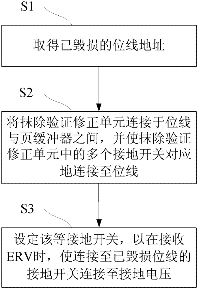
[0030] In order to fully understand the purpose, features and effects of the present invention, the present invention will be described in detail through the following specific embodiments and accompanying drawings, as follows.

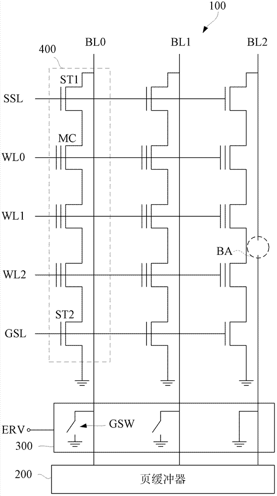
[0031] See first figure 1 , is a circuit block diagram of the NAND flash memory device in the semiconductor device of the embodiment of the present invention when it is in the erase verification state. The present invention takes a NAND flash memory device as an example, and other types of semiconductor devices, such as semiconductor devices such as transistors, are applicable to the device structures or methods proposed in the embodiments of the present invention.

[0032] figure 1 The memory cell array 100 of the present invention is an example of three NAND strings. In this example, each NAND string 400 includes a string selection transistor ST1, a ground selection transistor ST2, and three memory cells MC.

[0033] The memory cell array 100 incl...


PUM


Abstract

The invention discloses a semiconductor device and a method for accelerating an erase verification procedure by the same. An erase verification correction unit is connected between a damaged bit line in the semiconductor device and a page buffer; through a special line arrangement on the damaged bit line, a grounding switch of the erase verification correction unit can connect the damaged bit line to a grounding voltage during an erase verification procedure, so that the page buffer can receive the grounding voltage to further verify that the damaged bit line has passed the erase verification, thereby substantially saving repeated verification time consumed in the prior art.

Description

technical field [0001] The present invention relates to a semiconductor device, and more particularly to a semiconductor device capable of accelerating an erase verification procedure. Background technique [0002] In flash memory devices, a verify operation is necessary to confirm that the charge is properly injected into the memory cell by the programming operation. If the verification operation fails, the programmed operation and the verification operation will be repeated until the result of the verification operation is successful or a special condition is met (for example, when repeated 100 times and still fails). [0003] In an erase operation, a verify operation is similarly performed to confirm that charge is properly removed from the memory cell. Erase verification usually precharges the bit line to a voltage level, the erased memory cell will discharge the bit line, and the page buffer connected to the bottom of the bit line will verify whether the bit line is di...

Claims


Application Information

Patent Timeline
IPC IPC(8): G11C7/10G11C7/12
Inventor 陈敦仁
Owner EON SILICON SOLUTION
Why Eureka
Try Eureka