Wafer prealignment control method

A control method and pre-alignment technology, applied in the field of IC manufacturing and computer control, which can solve the problems of irregular gaps, not found, too many iterations, etc.

Inactive Publication Date: 2013-07-10
SHENYANG SIASUN ROBOT & AUTOMATION
View PDF4 Cites 14 Cited by
  • Summary
  • Abstract
  • Description
  • Claims
  • Application Information

AI Technical Summary

Problems solved by technology

The disadvantage of this method is that the geometric distance of the center of the notch calculated before and after is used as the judgment condition for the termination of the iteration during the fitting iteration. Since the radius of the notch center may be large or the notch is irregular, this will lead to too many iterations or no satisfying condition. The result of judging the conditions, and it is also necessary to sample the edge of the wafer twice, which is not efficient

Method used


Image

  • Wafer prealignment control method
  • Wafer prealignment control method
  • Wafer prealignment control method

Examples


Embodiment Construction

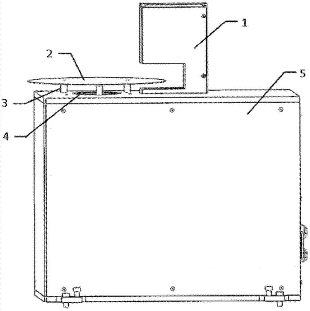
[0044] see figure 1 , in a preferred embodiment of the present invention, a wafer center pre-alignment equipment includes a control cabinet 5 for controlling the pre-aligned wafer 4; a top seat 3 for pre-aligning the wafer 4 The wafer 4 was previously supported; a negative pressure adsorption rotating device 4 provided on the control cabinet 5 is used to lift up the wafer 2 and extract the air between the tray and the wafer 2 to form a vacuum state , and drive the wafer 2 to rotate at the same time; a sensor 1 arranged on the control cabinet 5 is used to collect edge data of the wafer 4 and obtain the speed information of the corresponding negative pressure adsorption rotating device 4 . In one embodiment, the sensor is a single CCD sensor for collecting data at the edge of the wafer 2 .

[0045] The negative pressure adsorption rotating device 4 has a rotation center. The maximum range of the sensor 1 is L, and the distance from the maximum range to the negative pressure ad...


PUM


Abstract

A wafer prealignment control method comprises the following steps: a first step of providing a negative pressure absorption rotating device for pumping air between a tray and a wafer to form a vacuum state and driving the wafer to rotate, and a second step of providing a sensor used for collecting edge data of the wafer and recording rotating speed information of the rotating device. The wafer prealignment control method further comprises wafer positioning and wafer notch positioning, wherein the wafer positioning comprises the following steps: a first step of data acquisition, a second step of data preprocessing, and a third step of circle fitting to find the circle center position of the wafer. The wafer notch positioning comprises the following steps: a first step of notch coarse positioning, a second step of notch fitting, a third step of an iteration termination, a fourth step of finding a coordinate of the center according to the notch edge center, and the position and the angle of the wafer are adjusted.

Description

technical field [0001] The invention relates to the field of computer control, in particular to a wafer pre-alignment control method in the field of IC manufacturing. Background technique [0002] Wafer pre-alignment control is one of the most important links in the IC manufacturing process. Specifically, the process of wafer pre-alignment control is to use a certain method to make the center of the wafer within a certain range, and at the same time, the notch of the wafer stays at a specified angle, which includes two steps: center positioning and notch detection. main process. [0003] In the existing technology, the patent name is silicon wafer pre-alignment control method, and the publication number is CN100355055C. A linear array CCD sensor is used to sample the edge data of the wafer to find out the approximate position of the notch. Secondary fine sampling is performed on the edge data of the notch, and the center coordinates of the notch are obtained by fitting the...

Claims


Application Information

Patent Timeline
Patent Type & Authority Applications(China)
IPC IPC(8): H01L21/68
Inventor 徐方曲道奎贾凯邹风山宋吉来刘晓帆李邦宇李崇
Owner SHENYANG SIASUN ROBOT & AUTOMATION
Why Eureka
Try Eureka