

Asymmetric pressing control slab warping structure of multilayer printed circuit board
A multi-layer printing and circuit board technology, applied in the direction of printed circuit components, etc., can solve the problems of multi-layer printed circuit board board warping, and achieve the effect of reducing board warping
Inactive Publication Date: 2013-07-10
竞陆电子(昆山)有限公司
View PDF0 Cites 4 Cited by
- Summary
- Abstract
- Description
- Claims
- Application Information
AI Technical Summary
Problems solved by technology
[0002] In the prior art, the adjacent layers of multilayer printed circuit boards are generally bonded together by PP (polypropylene) adhesive layers, specifically, a whole sheet of PP is stacked between adjacent layers, Then, the adjacent layers are bonded together by PP by thermal pressing, and all the PP adhesive layers are of the same thickness. Since the materials of each layer have different expansion and contraction properties, the multilayer printed circuit board of this structure is easy There is a warping problem
Method used
View moreImage
Smart ImageViewing Examples


Examples
Embodiment
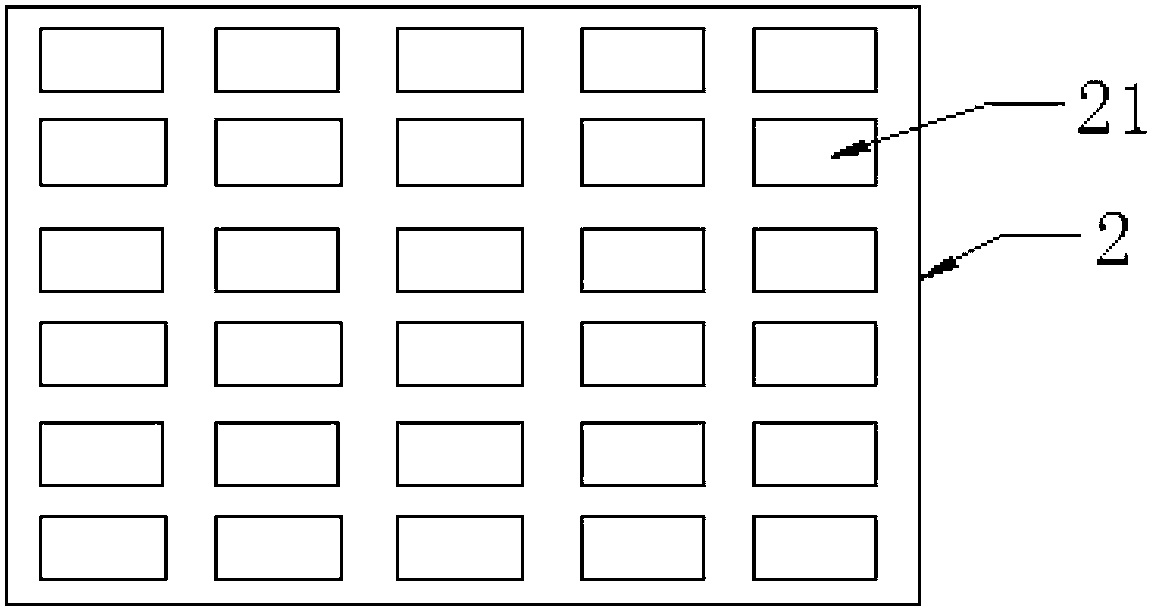
[0013] Embodiment: an asymmetric lamination control board warping structure of a multi-layer printed circuit board. There is a film layer 2 between adjacent circuit layers 1. The film layers from the top circuit layer to the center circuit layer are sorted in sequence, and the The film layers between the bottom line layer and the center line layer are sorted in order, and the two film layers with the same serial number are defined as relative film layers, and the thicknesses of the two film layers of each pair of opposite film layers are different, and the film layers of each layer There are several hollowed-out parts 21 .
Login to View More PUM
 Abstract
The invention discloses an asymmetric pressing control slab warping structure of a multilayer printed circuit board. A film layer is arranged between every two adjacent line layers, the film layers between the top layer of line layer and the central line layer are sequenced, the film layers between the bottom layer of line layer and the central line layer are sequenced, two film layers with the same sequence number are defined as relative film layers, the thicknesses of the two films layers in each pair of relative film layers are different, and each film layer is provided with a plurality of hollow parts. The asymmetric pressing control slab warping structure of the multilayer printed circuit board is capable of reducing slab warping effectively, and the slab warping rate is controlled to be lower than 0.75%.
Description
technical field [0001] The invention belongs to the field of multilayer printed circuit board structures, and in particular relates to a pressing structure capable of effectively reducing board warping. Background technique [0002] In the prior art, the adjacent layers of multilayer printed circuit boards are generally bonded together by PP (polypropylene) adhesive layers. Specifically, a whole sheet of PP is stacked between adjacent layers. Then, the adjacent layers are bonded together by PP through thermal pressing, and all the PP adhesive layers are of the same thickness. Since the materials of each layer have different expansion and contraction properties, the multilayer printed circuit board of this structure is easy There is a board warping problem. Contents of the invention [0003] In order to overcome the above-mentioned defects, the present invention provides an asymmetric lamination control board warp structure of a multilayer printed circuit board, which can ...
Claims
Login to View More Application Information
Patent Timeline
 IPC IPC(8): H05K1/02
Inventor李泽清
Owner竞陆电子(昆山)有限公司