
Method for detecting flexible printed circuit after laser processing

A flexible circuit board and laser processing technology, applied in the direction of optical testing flaws/defects, etc., can solve the problem that the flexible circuit board cannot stick to the glass surface of the scanner, etc., to achieve the effect of improving accuracy and good technical effect

Active Publication Date: 2013-07-24
KUNSHAN THETA MICRO
View PDF1 Cites 1 Cited by
  • Summary
  • Abstract
  • Description
  • Claims
  • Application Information

AI Technical Summary

Problems solved by technology

[0007] The technical problem to be solved by the present invention is the problem that the flexible circuit board cannot cling to the glass surface of the scanner when the flexible circuit board is detected after laser processing in the prior art

Method used


Image

  • Method for detecting flexible printed circuit after laser processing
  • Method for detecting flexible printed circuit after laser processing
  • Method for detecting flexible printed circuit after laser processing

Examples


Embodiment 1

[0040] A detection method after laser processing of a flexible circuit board, comprising the following steps:

[0041] a) Take the flexible circuit board after laser processing, fix it with an adsorption light box, and put it on the working platform for scanner detection;

[0042] b) Use a linear ccd device combined with a stepper motor to scan line by line to obtain the image of the soft board;

[0043] c) Through the recognition algorithm, the openings and lines in the image are converted into graphics;

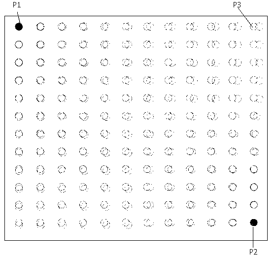
[0044] d) Set P1 and P2 two-point graphic marks on the two opposite corners of the soft board, and carry out two-point initial alignment through the P1 and P2 graphic marks;

[0045] e) Set the range of a parameter D, which represents the minimum value Dmin and the maximum value Dmax of the deviation distance between the design graphic center and the corresponding identified graphic center position, where both Dmin and Dmax are greater than 0;

[0046] f) Starting from po...

Embodiment 2

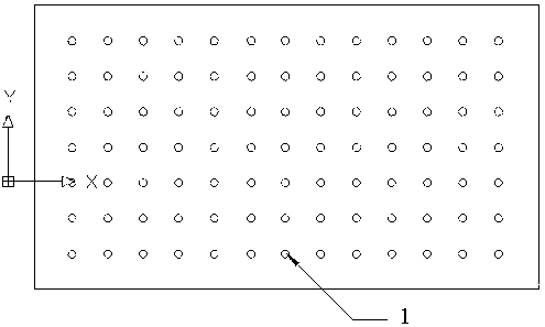
[0056] An adsorption light box for detection after laser processing of flexible circuit boards, including a glass surface, the glass surface has small holes in a dot matrix, and a suction device is provided on the side close to the glass surface in the light box, placed on the glass surface of the light box The flexible circuit board can be adsorbed on the glass surface under the suction state of the suction device.

[0057] Make a lattice of small holes on the glass surface of the light box, and at the same time ensure the smoothness and flatness of the lattice surface on the glass surface; install an air suction device on the side of the added glass, such as image 3 , 4 As shown, the flexible circuit board on the glass surface of the light box can be tightly adsorbed on the glass under the suction state, and at the same time, the place other than the flexible circuit board of the light box needs to be covered with white paper (the edge of the white paper overlaps with the f...

Embodiment 3

[0060] A flexible board self-adaptive multiple alignment detection method, such as Figure 6 , Figure 7 As shown, it includes the following steps: using a linear ccd device combined with a stepping motor to scan progressively to obtain an image of the soft board; using a recognition algorithm to convert the openings and lines in the image into graphics;

[0061] Set P1 and P2 graphic marks on the two diagonal vertex positions of the soft board, and perform two-point initial alignment through the P1 and P2 graphic marks; set a parameter D range, which represents the center of the design graphic and the corresponding recognized graphic The minimum value Dmin and the maximum value Dmax of the center position deviation distance, where both Dmin and Dmax are greater than 0;

[0062] Starting from point P1, according to a certain recognition order, identify the openings and lined graphics of the soft board one by one; when the position deviation between the center of the current r...


PUM


Abstract

The invention relates to a method for detecting a flexible printed circuit after laser processing. The method mainly solves the problem that based on the prior art, in laser processing on a flexible printed circuit, the flexible printed circuit cannot press close to a glass surface of a scanner. The method is characterized in that before detection, a fixing process adopts an adsorption-type light box; the adsorption-type light box comprises a glass surface; the glass surface is provided with dot-matrix small apertures; a side in the adsorption-type light box close to the glass surface is provided with an air suction device; and a flexible printed circuit on the glass surface of the adsorption-type light box can be adsorbed on the glass surface under air suction of the air suction device. The method solves the above problem well and can be used for a laser processing industry.

Description

[0001] technical field [0002] The invention relates to a detection method after laser processing of a flexible circuit board. Background technique [0003] In the laser processing (cutting, drilling, etc.) industry, high-precision scanners can be used to scan processed products, such as figure 1 As shown, placing a light box on the scanner can achieve a better image effect, and then compare the obtained high-resolution image with the CAD file through the software. The software can realize the vectorized recognition of the opening in the image. After selecting two points (or several points) for alignment, the opening in the CAD can be compared with the opening identified on the image one by one, and the position accuracy and the size of the opening can be checked. qualified. For rigid products, such as steel sheets, the detection effect is very good. However, when testing flexible circuit boards, its flexibility causes the flexible board to not be close to the glass surfa...

Claims


Application Information

Patent Timeline
Patent Type & Authority Applications(China)
IPC IPC(8): G01N21/88
Inventor 魏志凌宁军龚关吉剑青
Owner KUNSHAN THETA MICRO
Learn More