PCB and film alignment device

A film alignment and PCB board technology, which is applied to instruments, printed circuits, photoengraving processes of patterned surfaces, etc., can solve the problems of low alignment efficiency and low alignment accuracy, achieve stable positioning and improve alignment efficiency. , to ensure the effect of alignment accuracy

Active Publication Date: 2013-08-07
GOERTEK INC
View PDF5 Cites 24 Cited by
  • Summary
  • Abstract
  • Description
  • Claims
  • Application Information

AI Technical Summary

Problems solved by technology

[0003] The technical problem to be solved by the present invention is to provide a PCB board and film alignment device to solve the problems of low alignment accuracy and low alignment efficiency in the prior art

Method used


Image

  • PCB and film alignment device
  • PCB and film alignment device
  • PCB and film alignment device

Examples


Embodiment Construction

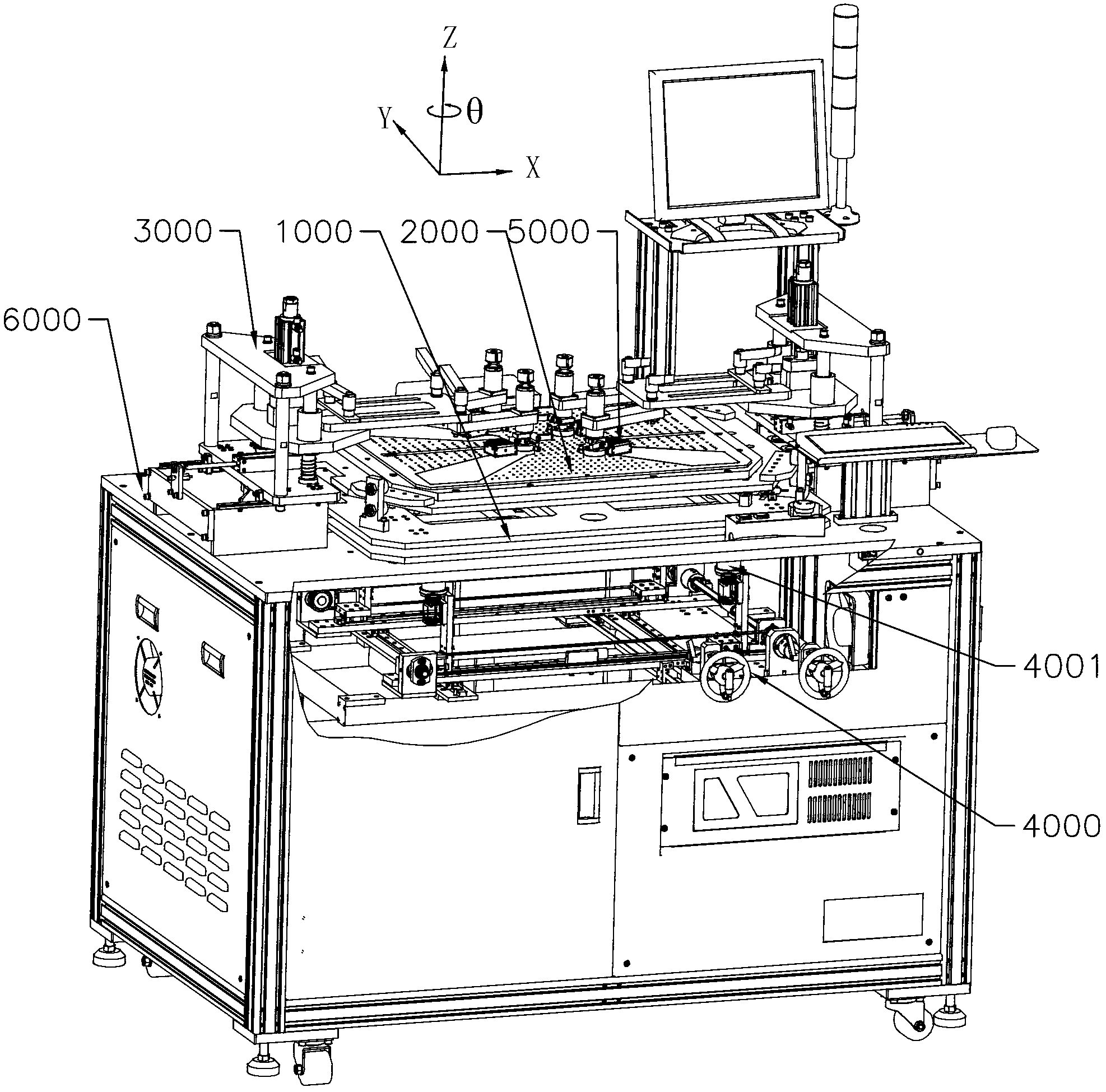
[0036] Such as figure 1 As shown, a PCB board and film alignment device. See X, Y, Z, θ directions in the three-dimensional coordinate system figure 1 , where the X direction and the Y direction are two directions perpendicular to each other in the horizontal plane, the Z direction is the direction perpendicular to the horizontal plane, and the θ angle rotation direction is the direction of rotation around the Z direction.

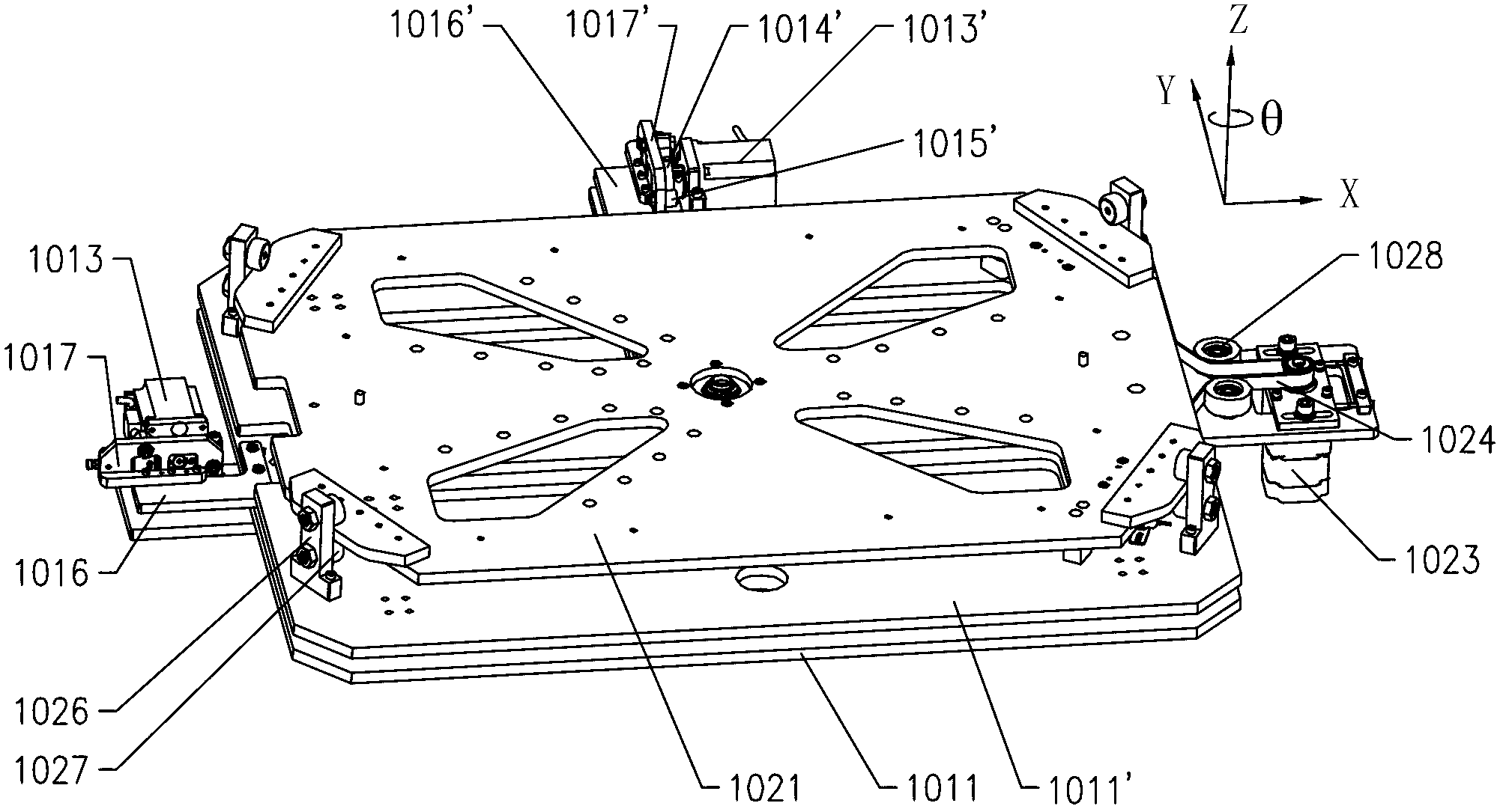
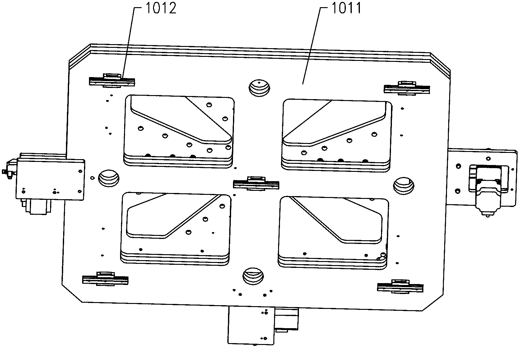
[0037] The PCB board and film alignment device includes a frame, and the following parts installed on the frame: X-Y-θ three-degree-of-freedom adjustment mechanism 1000; fixed on the X-Y-θ three-degree-of-freedom adjustment mechanism 1000 for adsorption PCB board The rectangular vacuum adsorption platform 2000, the X-Y-θ three-degree-of-freedom adjustment mechanism 1000 controls the translation and rotation of the vacuum adsorption platform 2000 along the X and Y directions, and the four corners of the vacuum adsorption platform 2000 extend diagonally. L...


PUM


Abstract

The invention discloses a PCB (printed circuit board) and film alignment device, which comprises a rack and the following parts installed on the rack: an X-Y-theta three-freedom degree adjustment mechanism; a rectangular vacuum adsorption platform fixed on the X-Y-theta three-freedom degree adjustment mechanism and used for PCB adsorption, with light transmitting parts disposed at four corners of the vacuum adsorption platform and extending along diagonal lines; two two-point compression mechanisms arranged over the vacuum adsorption platform relatively; four CCD lens that are mounted below the X-Y-theta three-freedom degree adjustment mechanism, read alignment marks at four corners of the PCB and the film through the light transmitting parts, are in rectangular arrangement and mounted on one spacing adjustment mechanism, and are in connection with a controller, the control end of which is connected to the X-Y-theta three-freedom degree adjustment mechanism; and light sources for providing illuminance conditions for the four CCD lens. The alignment device disclosed in the invention improves the alignment accuracy and alignment efficiency.

Description

technical field [0001] The invention relates to a PCB board and film aligning device used in the PCB board manufacturing process. Background technique [0002] In the PCB board manufacturing process, the PCB board and the film need to be aligned before exposure, and then the aligned PCB board and film are put into the exposure machine for exposure. In the prior art, pins are generally used for alignment, and alignment holes are punched out at the corresponding positions of the PCB board and the film, and then the alignment operation of the two is realized by putting the alignment holes on the pins. In the above-mentioned alignment structure, since the diameter of the alignment hole cannot be completely equal to the outer diameter of the pin, the alignment accuracy of the two will inevitably be low, and manual alignment is required, which is inefficient. Contents of the invention [0003] The technical problem to be solved by the present invention is to provide a PCB board...

Claims


Application Information

Patent Timeline
Patent Type & Authority Applications(China)
IPC IPC(8): G03F9/00H05K3/00
Inventor 苏斌贺文佳于浩于涛徐友瑞王克生
Owner GOERTEK INC
Why Eureka
Try Eureka