Supercharge Your Innovation With Domain-Expert AI Agents!

cmos sensor array

A technology of CMOS sensors and capacitors, which is applied to TVs, color TV parts, electrical components, etc., and can solve problems such as unbalanced shooting and response of CMOS image sensors

Active Publication Date: 2018-01-26
TAIWAN SEMICON MFG CO LTD
View PDF4 Cites 0 Cited by
  • Summary
  • Abstract
  • Description
  • Claims
  • Application Information

AI Technical Summary

Problems solved by technology

However, not all source followers in the pixel array have the same gain, which results in an unbalanced photoresponse of the CMOS image sensor

Method used


Image

  • cmos sensor array
  • cmos sensor array
  • cmos sensor array

Examples


Embodiment Construction

[0029] This description of the exemplary embodiments is intended to be read in conjunction with the accompanying drawings, which are to be considered a part of this fully written specification.

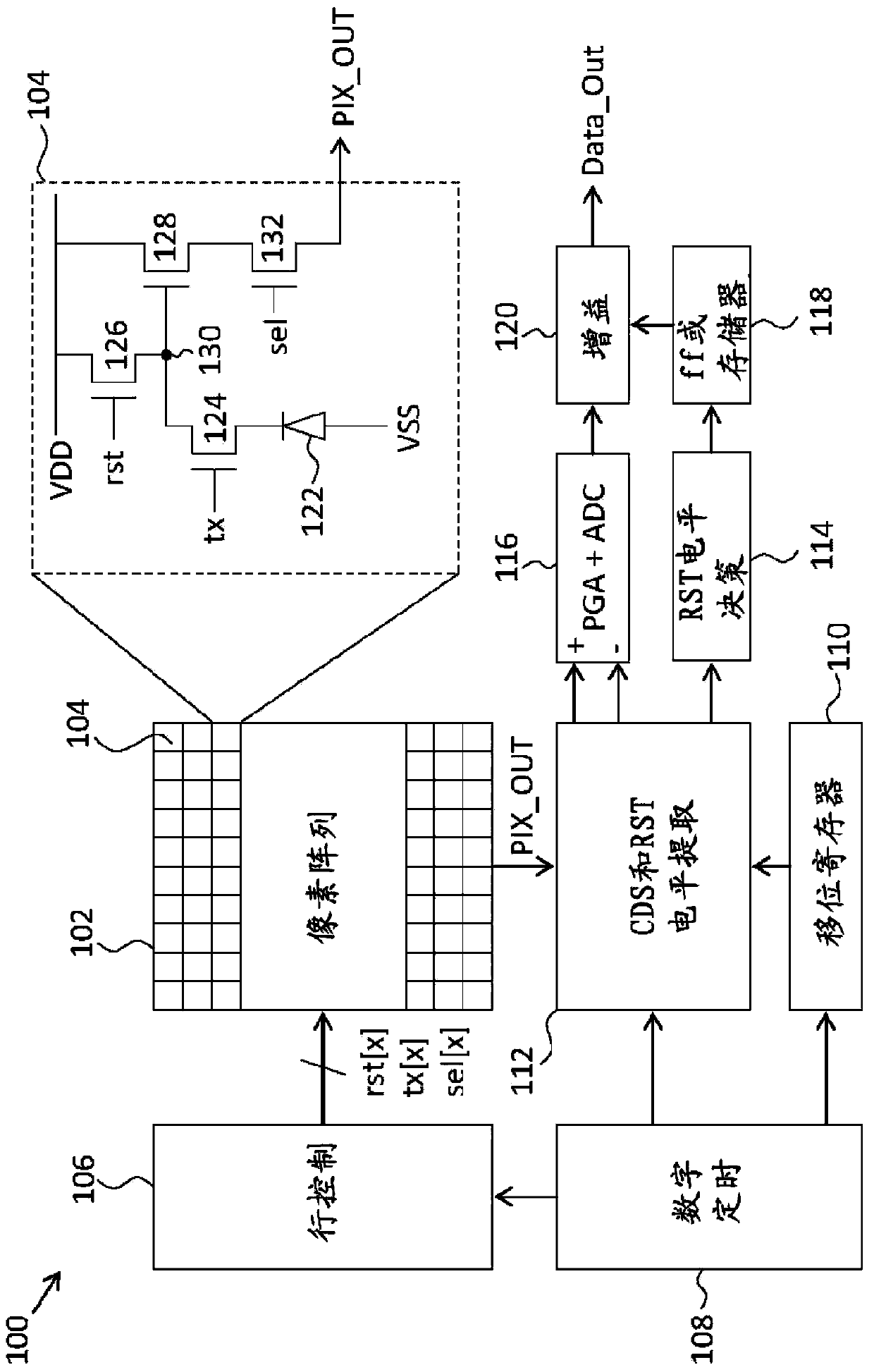
[0030] Some embodiments of the improved CMOS sensor array described herein advantageously determine the pixel reset voltage level of the CMOS pixel and adjust the gain of the output data based on the pixel reset voltage level. In some embodiments, adjusting the gain based on the detected pixel reset voltage level reduces source follower gain variation across the array, thereby reducing fixed pattern noise (“FPN”) and minimizing shot response non-uniformity ( "PRNU").

[0031] figure 1 One example of an improved CMOS imaging device 100 comprising an array 102 of CMOS pixels 104 is shown. The row control circuit 106 provides control signals such as reset signals rst[X], tx[x] and a row selection signal sel[x] to the pixel array 102 for controlling the readout of data from the array 10...


PUM


Abstract

A CMOS sensor includes: pixels configured to output voltages based on incident light received by the pixels. A first circuit is connected to the pixel and configured to determine a reset voltage for the pixel. The second circuit is connected to the first circuit and is configured to select a gain value based on a reset voltage of the pixel. A gain circuit is connected to the second circuit and configured to set a voltage level of gain selected by the second circuit. The invention also provides a CMOS sensor array.

Description

technical field [0001] The disclosed systems and methods relate to integrated circuits. More particularly, the disclosed systems and methods relate to integrated circuits for image sensors. Background technique [0002] Complementary metal oxide semiconductor (CMOS) image sensors convert images into electrical signals. Such sensors are found in digital cameras or other electronic devices used for imaging. CMOS image sensors usually use source followers as isolation devices. In particular, source followers are used to drive analog signals from individual pixel cells to shared column lines. However, not all source followers in the pixel array have the same gain, which leads to unbalanced photoresponse of the CMOS image sensor. Contents of the invention [0003] According to one aspect of the present invention, there is provided a CMOS sensor comprising: a pixel configured to output a voltage based on incident light received by the pixel; a first circuit connected to the ...

Claims


Application Information

Patent Timeline
Patent Type & Authority Patents(China)
IPC IPC(8): H04N5/374H04N5/3745H04N5/378
CPCH04N25/671H04N25/78H04N25/75
Inventor 周国煜赵亦平涂宏益周伯圣陈怡哲
Owner TAIWAN SEMICON MFG CO LTD
Features
  • R&D
  • Intellectual Property
  • Life Sciences
  • Materials
  • Tech Scout
  • Unparalleled Data Quality
  • Higher Quality Content
  • 60% Fewer Hallucinations
Learn More