A component slotting structure and pcb
A component and step-type technology, applied in the field of electronics, can solve the problems of rising impedance of the output end of the power tube and short-circuiting of the flange, so as to avoid the short-circuit of the ignition and reduce the impact.
- Summary
- Abstract
- Description
- Claims
- Application Information
AI Technical Summary
Problems solved by technology
Method used
Image

Examples
Embodiment 1
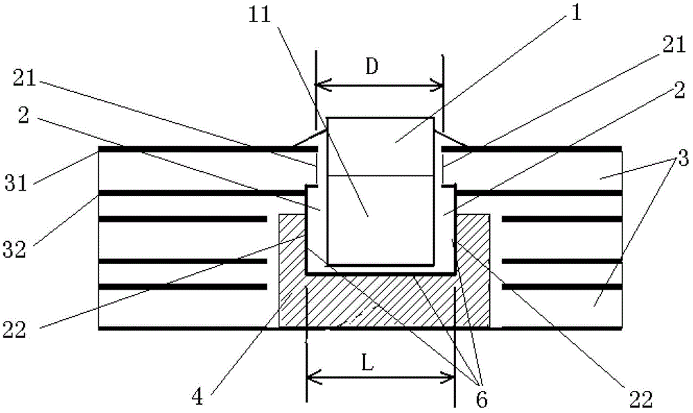
[0033] Such as figure 1 As shown, the embodiment of the present invention provides a slotted structure of a component 1, the slotted structure of a component 1 is arranged on a PCB, and the slotted structure of a component 1 includes a stepped slot 2 and an electroplating layer 6, The stepped slot 2 is used to accommodate the components 1, the lower part 22 of the inner wall of the stepped slot 2 is wider than the upper part 21, and the connection between the upper part 21 and the lower part 22 is lower than the PCB. The top metal layer 31, and the connection is not lower than the second metal layer 32 of the PCB, and the electroplating layer 6 is closely arranged along the inner wall of the stepped groove 2 except the upper part 21 , the component 1 is electrically connected to the second metal layer 32 through the electroplating layer 6 .
[0034] Wherein, the opening size L of the lower part 22 of the inner wall of the stepped groove 2 is larger than the opening size D of ...
Embodiment 2
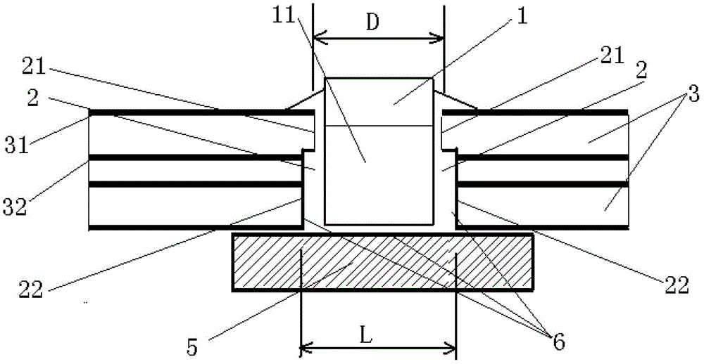
[0041] Such as figure 2 As shown, the embodiment of the present invention provides a slotted structure of a component 1, the slotted structure of a component 1 is arranged on a PCB, and the slotted structure of a component 1 includes a stepped slot 2 and an electroplating layer 6, The stepped slot 2 is used to accommodate the components 1, the lower part 22 of the inner wall of the stepped slot 2 is wider than the upper part 21, and the connection between the upper part 21 and the lower part 22 is lower than the PCB. The top metal layer 31, and the connection is not lower than the second metal layer 32 of the PCB, and the electroplating layer 6 is closely arranged along the inner wall of the stepped groove 2 except the upper part 21 , the component 1 is electrically connected to the second metal layer 32 through the electroplating layer 6 .
[0042] Specifically, as a preference, such as figure 2 As shown, the slotted structure of the component 1 also includes a substrate ...
Embodiment 3
[0050] An embodiment of the present invention provides a PCB, and the PCB is provided with the component slot structure in the above two embodiments. The embodiment of the present invention is the same as the slotting structure of the components in all the above embodiments, and will not be repeated here. The embodiment of the present invention prevents the flange of the power tube from directly sparking and short circuiting with the top metal layer and reduces the impact on the performance of the output end of the power tube.
[0051] The serial numbers of the above embodiments of the present invention are for description only, and do not represent the advantages and disadvantages of the embodiments.
PUM
 Abstract
Description
Claims
Application Information
 - R&D Engineer
- R&D Manager
- IP Professional
- Industry Leading Data Capabilities
- Powerful AI technology
- Patent DNA Extraction
Browse by: Latest US Patents, China's latest patents, Technical Efficacy Thesaurus, Application Domain, Technology Topic.
© 2024 PatSnap. All rights reserved.Legal|Privacy policy|Modern Slavery Act Transparency Statement|Sitemap