Slot structure for component and PCB (printed circuit board)

A technology of components and electroplating layer, which is applied in the electronic field, can solve problems such as the increase of impedance at the output end of the power tube and the short circuit of the flange ignition, so as to avoid the short circuit of the ignition and reduce the effect of the impact

Active Publication Date: 2013-09-11
HUAWEI MACHINERY
View PDF3 Cites 10 Cited by
  • Summary
  • Abstract
  • Description
  • Claims
  • Application Information

AI Technical Summary

Problems solved by technology

[0007] In order to solve the problems in the prior art that the flange is easy to be directly connected to the top metal layer and short-circuited by ignition, and the impedance of the output end of the power tube increases, the embodiment of the present invention provides a component slotting structure and a PCB

Method used


Image

  • Slot structure for component and PCB (printed circuit board)
  • Slot structure for component and PCB (printed circuit board)

Examples


Embodiment 1

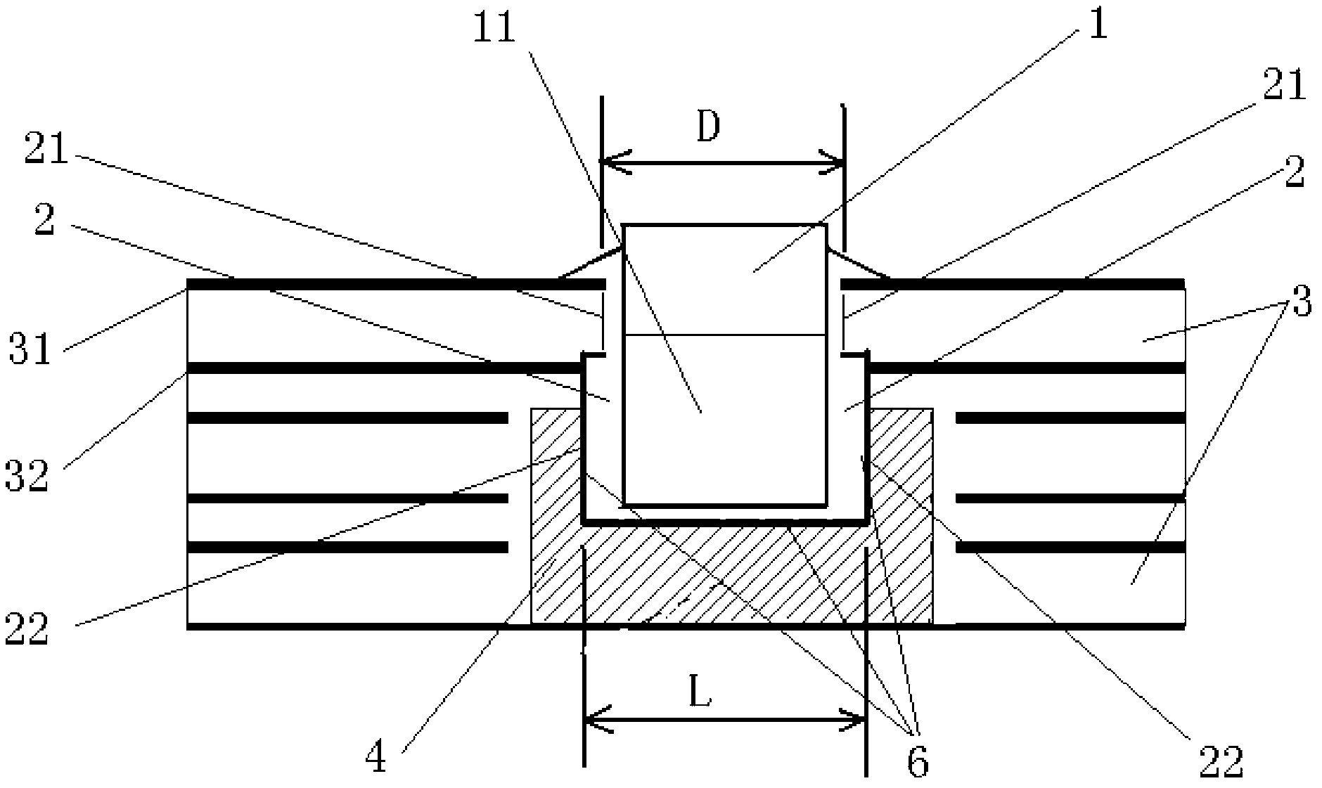
[0033] Such as figure 1 As shown, the embodiment of the present invention provides a slotted structure of a component 1, the slotted structure of a component 1 is arranged on a PCB, and the slotted structure of a component 1 includes a stepped slot 2 and an electroplating layer 6, The stepped slot 2 is used to accommodate the components 1, the lower part 22 of the inner wall of the stepped slot 2 is wider than the upper part 21, and the connection between the upper part 21 and the lower part 22 is lower than the PCB. The top metal layer 31, and the connection is not lower than the second metal layer 32 of the PCB, and the electroplating layer 6 is closely arranged along the inner wall of the stepped groove 2 except the upper part 21 , the component 1 is electrically connected to the second metal layer 32 through the electroplating layer 6 .

[0034] Wherein, the opening size L of the lower part 22 of the inner wall of the stepped groove 2 is larger than the opening size D of ...

Embodiment 2

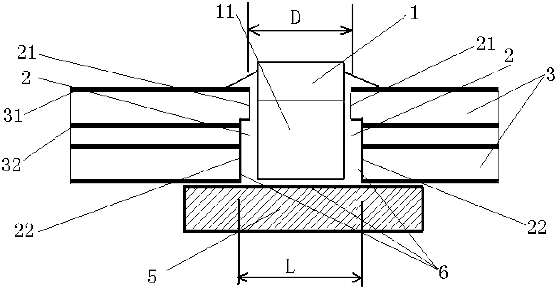
[0041] Such as figure 2 As shown, the embodiment of the present invention provides a slotted structure of a component 1, the slotted structure of a component 1 is arranged on a PCB, and the slotted structure of a component 1 includes a stepped slot 2 and an electroplating layer 6, The stepped slot 2 is used to accommodate the components 1, the lower part 22 of the inner wall of the stepped slot 2 is wider than the upper part 21, and the connection between the upper part 21 and the lower part 22 is lower than the PCB. The top metal layer 31, and the connection is not lower than the second metal layer 32 of the PCB, and the electroplating layer 6 is closely arranged along the inner wall of the stepped groove 2 except the upper part 21 , the component 1 is electrically connected to the second metal layer 32 through the electroplating layer 6 .

[0042] Specifically, as a preference, such as figure 2 As shown, the slotted structure of the component 1 also includes a substrate ...

Embodiment 3

[0050] An embodiment of the present invention provides a PCB, and the PCB is provided with the component slot structure in the above two embodiments. The embodiment of the present invention is the same as the slotting structure of the components in all the above embodiments, and will not be repeated here. The embodiment of the present invention prevents the flange of the power tube from directly sparking and short circuiting with the top metal layer and reduces the impact on the performance of the output end of the power tube.

[0051] The serial numbers of the above embodiments of the present invention are for description only, and do not represent the advantages and disadvantages of the embodiments.


PUM


Abstract

The invention discloses a slot structure for a component and a PCB (printed circuit board). The slot structure comprises a stepped slot and an electroplated layer. The stepped slot is used for accommodating the component, the lower portion of the inner wall of the stepped slot is wider than the upper portion of the inner wall of the stepped slot, the joint between the upper portion and the lower portion of the inner wall of the stepped slot is lower than a top metal layer of the PCB and is not lower than a second metal layer of the PCB, the electroplated layer clings to parts, except for the upper portion of the stepped slot, of the inner wall of the stepped slot, and the component is electrically connected with the second metal layer by the electroplated layer. The slot structure for the component is arranged on the PCB. The slot structure and the PCB have the advantages that the lower portion of the inner wall of the stepped slot for accommodating the component is wider than the upper portion of the inner wall of the stepped slot, so that soldering tin accommodating space of the lower portion of the inner wall of the stepped slot is large, the climbing height of soldering tin along the inner wall of the stepped slot is reduced, and short circuit between the component and the top metal layer is prevented; the quantity of hollowed-out media between the top metal layer and the second metal layer of the PCB is low, so that decrease of an effective dielectric constant of the PCB is not obvious, and influence on the impedance of an output end of the component is low.

Description

technical field [0001] The invention relates to the field of electronics, in particular to a component slotting structure and a PCB. Background technique [0002] The complexity of power amplifier control circuit design has led to an increase in the application of multi-layer power amplifier boards. In order to save costs, PCB (Printed circuit board printed circuit board) generally adopts a structure of high-frequency plate mixed pressure. Among them, components are installed on the PCB, components There is a flange on the top, and the components are connected to the reference ground of the matching junction / microstrip line through the flange, that is, connected to the second metal layer of the PCB to form a loop. The actual design needs to shorten the flange and the second metal layer of the PCB as much as possible. return path between the two. [0003] At present, the industry mainly adopts the following scheme: first mill out the slot for the component position on the PC...

Claims


Application Information

Patent Timeline
IPC IPC(8): H05K1/18
Inventor 黄明利李松林曹曦
Owner HUAWEI MACHINERY
Why Eureka
Try Eureka