Supercharge Your Innovation With Domain-Expert AI Agents!

Address transition detection circuit and method

A detection circuit and address conversion technology, applied in information storage, static memory, digital memory information, etc., can solve problems such as large chip area

Active Publication Date: 2013-09-18
MACRONIX INT CO LTD
View PDF4 Cites 0 Cited by
  • Summary
  • Abstract
  • Description
  • Claims
  • Application Information

AI Technical Summary

Problems solved by technology

Therefore, all minimum delay units 106 in this circuit need to occupy a larger chip area

Method used


Image

  • Address transition detection circuit and method
  • Address transition detection circuit and method
  • Address transition detection circuit and method

Examples


Embodiment Construction

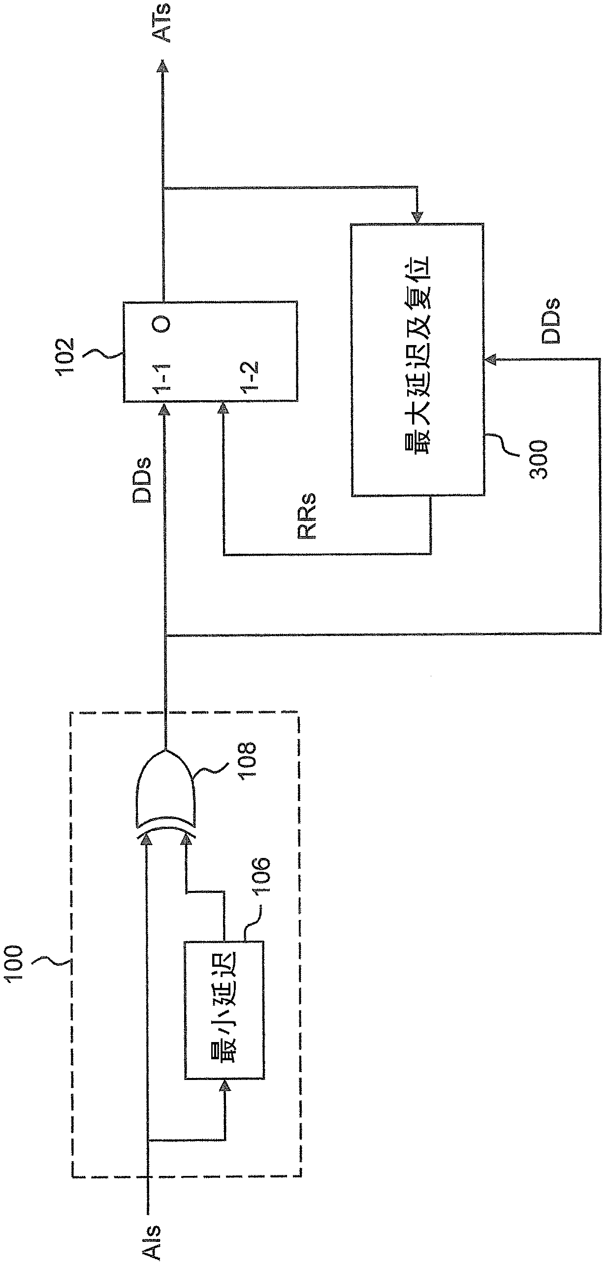
[0047] The invention discloses a signal detection circuit suitable for detecting address transitions on multiple address signal lines in a memory device. The circuit can also be used to detect transitions of other signals such as die select control signals or die enable control signals.

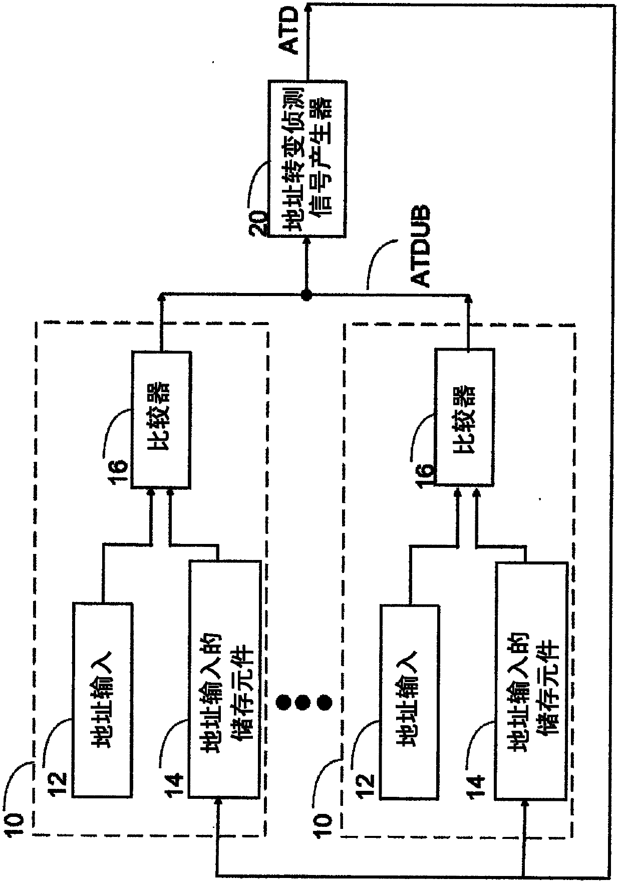
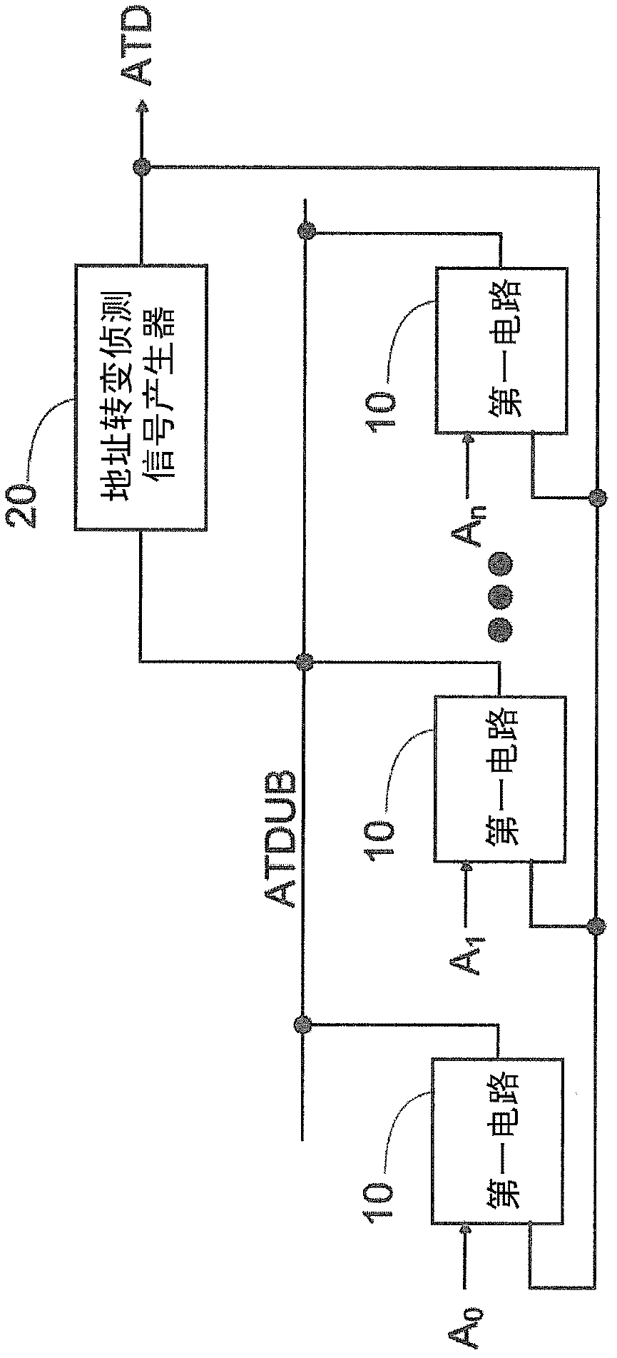
[0048] figure 2 A block schematic diagram of an embodiment of the invention is shown. The block diagram includes a plurality of first circuits 10 corresponding to a plurality of address signal lines, and an address transition detection signal (ATD) generator 20 (second circuit). Each first circuit 10 includes a comparator 16 which compares an input address at the address input 12 with the stored address in the storage element 14 . The address input 12 includes a signal line corresponding to an address signal line, such as a signal line connected to an input pin of an integrated circuit or a line connected to an address generator in an integrated circuit. For example, a 32-pin packaged mem...


PUM


Abstract

The invention discloses an address transition detection circuit and method. The address transition detection circuit is used in a bus including a plurality of address signal lines and comprises a first circuit and a second circuit of each address signal line. Each first circuit has a first input a second input and an output; the first input is coupled with one address signal line, and the second input is coupled with an address transition detection signal. The first circuit stores current level of the first input to respond to an address transition detection pulse of the address transition detection signal and generates output by comparing current input level with the level stored by the first input. The second circuit has an input and an output and receives a transition signal from the first circuit. For response to the signal, the second circuit generates the address transition detection pulse of the address transition detection signal as output.

Description

technical field [0001] The present invention relates to digital circuits, and more particularly to address transition detection (ATD) circuits. Background technique [0002] An address transition detection (ATD) circuit for use with an address bus having any number of addresses is disclosed in U.S. Patent No. 5,875,152 entitled "address Transition Detection Circuit for a Semiconductor Memory Capable of Detecting Narrowly Spaced Address Change", issued in 1999 Announcement on February 23, 2019. This patent discloses a circuit with an address transition detection (ATD) circuit that detects every address transition and provides an address transition detection (ATD) circuit suitable for use with very large number addresses the address bus of the memory. Such as figure 1 As shown in , an edge detection unit 100 in the prior art includes a minimum delay unit 106 and a comparator 108 . The minimum delay unit 106 outputs the delayed input address signal (AI) to the comparator 10...

Claims


Application Information

Patent Timeline
IPC IPC(8): G11C8/18G11C7/22
Inventor 林永丰
Owner MACRONIX INT CO LTD
Features
  • R&D
  • Intellectual Property
  • Life Sciences
  • Materials
  • Tech Scout
  • Unparalleled Data Quality
  • Higher Quality Content
  • 60% Fewer Hallucinations
Learn More