Display device

a technology of liquid crystal display panel and display panel, which is applied in static indicating devices, instruments, non-linear optics, etc., can solve the problems of affecting the quality of the display panel, so as to reduce the manufacturing cost and reduce the material cost.

Active Publication Date: 2014-06-26
EI DU PONT DE NEMOURS & CO +2
View PDF4 Cites 191 Cited by
  • Summary
  • Abstract
  • Description
  • Claims
  • Application Information

AI Technical Summary

Benefits of technology

[0019]The present invention allows detection of the existence of the crack which may cause the problem before connecting the flexible wiring substrate. This makes it possible to omit the process subsequent to the crack detection for a defective product, thus reducing the manufacturing cost. The process for connecting the flexible wiring substrate to the defective panel is no longer necessary, thus further reducing the material cost.

Problems solved by technology

Manufacturing the liquid crystal display devices of medium and small sizes one by one is disadvantageous in terms of cost.
When the glass is subjected to fracture, a crack may occur in an area around the liquid crystal display panel.
If the panel has the small frame and wiring such as the leader is formed at the area around the edge of the liquid crystal display panel, the crack may disconnect the peripheral leader.
A large number of inspection terminals are required in accordance with all the inspections as described above, resulting in insufficient space for the terminal portion of the liquid crystal display panel.
Cracks exist in all the glass substrates.
The problem may occur when such crack develops to disconnect the wiring, or to deteriorate reliability of sealing between the TFT substrate 100 and the counter substrate 200.
As a result, the subject liquid crystal display panel is regarded as a defective product.
That is, the generally employed method is not capable of detecting the existence of the crack until the flexible wiring substrate 110 is connected.

Method used


Image

  • Display device
  • Display device
  • Display device

Examples


first example

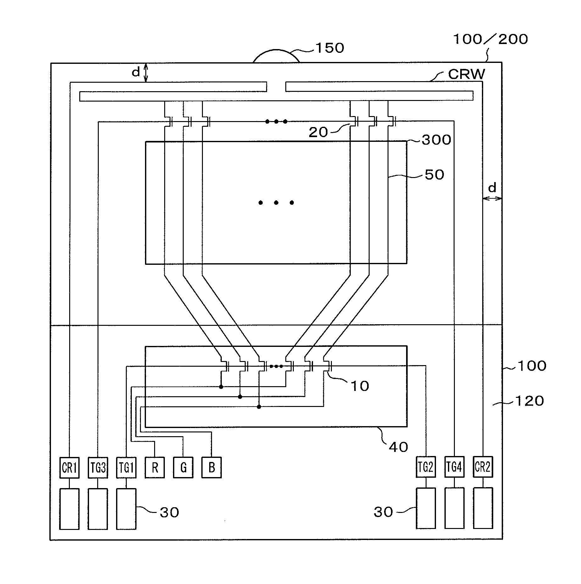
[0029]FIG. 1 schematically shows a crack detection circuit according to the example. Flexible wiring substrate terminals 30 for connecting the flexible wiring substrate 110 are provided at the outer side of inspection terminals CR1, CR2, TG1 and TG2, that is, at the lower part of the terminal portion 120 shown in FIG. 1. The terminal, wiring, circuit and the like shown in FIG. 1 for carrying out the lighting inspection are the same as those described referring to FIG. 8.

[0030]The lighting inspection is carried out by operating the lighting inspection switching transistor 10, red pixel terminal R, green pixel terminal G, blue pixel terminal B, the gate line for turning the lighting inspection switching transistor 10 on / off, the first test gate terminal TG1 and the second test gate terminal TG2. Like FIG. 8, the lighting inspection switching transistor 10 disposed at the same location as the IC driver 40 is formed on the TFT substrate 100, not on the IC driver 40.

[0031]Referring to FI...

second example

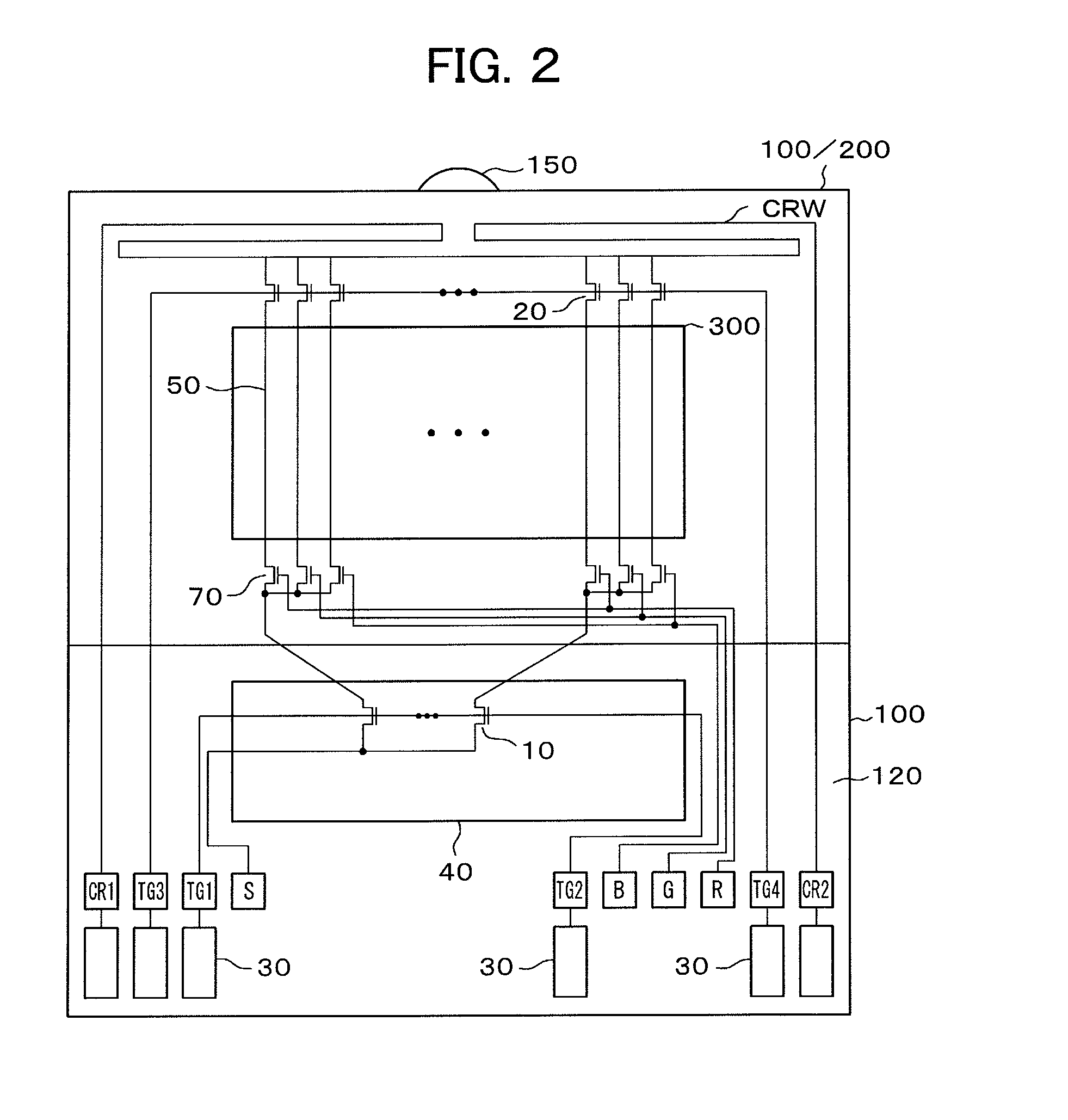
[0043]FIG. 2 schematically shows a crack detection circuit according to the second example of the present invention. The crack detection method according to the example is similar to that of the first example. This example is different from the first example in the method of displaying the image. Specifically, as definition of the screen becomes higher, the number of the video signal lines 50 is increased. Correspondingly, the number of leaders of video signal lines is increased as well, which causes the problem of the cost increase of the IC driver 40 and deteriorated reliability of the connection terminal owing to the increased terminals of the IC driver 40. Also the space of the terminal portion 120 which receives extended leaders of the video signal lines becomes insufficient.

[0044]As for the operation of the example, third switching transistors 70 are provided between the lighting inspection switching transistor 10 and the display region 300 to divide the single scanning period...

third example

[0048]FIG. 3 schematically shows a crack detection circuit according to the third example of the present invention. Basically, the crack detection method of this example is similar to the first example. The first example is configured to connect the gate of the crack inspection switching transistor 20 to the third test gate terminal TG3 and the fourth test gate terminal TG4. In this example, the third and the fourth test gate terminals do not exist. The gate of the crack inspection switching transistor 20 is connected to the red pixel terminal R which is connected to the source of the lighting inspection switching transistor 10.

[0049]This example is allowed to omit the third and fourth test gate terminals, thus saving the space of the terminal portion 120. When the crack inspection switching transistor 20 is turned on for crack detection, the ON signal is applied to the red pixel terminal R. At this time, the lighting inspection switching transistor 10 is in OFF state, which gives n...


PUM

PropertyMeasurementUnit
distanceaaaaaaaaaa
light transmittanceaaaaaaaaaa
sizesaaaaaaaaaa

Abstract

A display device is configured to provide a crack detection line running from a first crack detection terminal along a side of a TFT substrate to extend to a second crack detection terminal. A switching transistor for switching between an image display and crack detection is provided at a side opposite a terminal portion between the crack detection line and a video signal line. The crack that may cause disconnection in the crack detection line is detected by turning the switching transistor on, and applying the voltage for lighting inspection to the first crack detection terminal and the second crack detection terminal sequentially in this order.

Description

CLAIM OF PRIORITY[0001]The present application claims priority from Japanese Patent Application JP 2012-278310 filed on Dec. 20, 2012, the content of which is hereby incorporated by reference into this application.BACKGROUND[0002]The present invention relates to a display device, and more particularly, to a liquid crystal display device or an organic EL display device capable of detecting the degree of a crack in a cutting-plane line of a glass substrate, and an impact of the crack.[0003]The liquid crystal display device includes a TFT substrate having pixel electrodes and thin film transistors (TFT) formed in a matrix, and a counter substrate having a black matrix or an overcoat film formed at a location corresponding to the pixel electrode of the TFT substrate. The liquid crystal is interposed between the TFT substrate and the counter substrate. Images are formed by controlling light transmittance of the liquid crystal molecules for each pixel.[0004]Especially, the liquid crystal ...

Claims


Application Information

Patent Timeline
Patent Type & Authority Applications(United States)
IPC IPC(8): G02F1/13
CPCG02F1/1309G09G3/006G09G2300/0426G02F1/1339G02F1/136254
Inventor YANAGISAWA, SYOU
Owner EI DU PONT DE NEMOURS & CO
Why Eureka
Try Eureka