Display device and electronic equipment

a technology of electronic equipment and display device, which is applied in the field of display device, can solve the problems of difficulty in realizing large-scale and high-definition displays, devices are self-luminous, etc., and achieve the effects of reducing the amount of signal potential, reducing the amount of negative feedback to the pixel capacity, and reducing the drive curren

Active Publication Date: 2008-02-21
JOLED INC
View PDF7 Cites 199 Cited by
  • Summary
  • Abstract
  • Description
  • Claims
  • Application Information

AI Technical Summary

Benefits of technology

[0015]According to the embodiment of the invention, the correction of mobility of the drive transistor (mobility correction operation) is performed in the correction time from the first timing when the switching transistor turns on to the second timing when the sampling transistor turns off, after turning on the sampling transistor to start sampling of the signal potential. Specifically, the drive current flowing through the drive transistor in response to the signal potential is negatively fedback to the pixel capacity in the correction time and the signal potential held therein is adjusted. When the mobility of the drive transistor is larger, the amount of negative feedback is larger in response, the reduced amount of the signal potential increases, and thus, the drive current can be suppressed. On the other hand, when the mobility of the drive transistor is smaller, the amount of negative feedback to the pixel capacity is smaller and the reduced amount of the signal potential held therein is small. Therefore, the drive current is not reduced so much. In this manner, according to the magnitude of mobility of the drive transistors of the independent pixels, the signal potentials are adjusted to cancel the variations. Therefore, despite the variations in mobility of the drive transistors of the independent pixels, the independent pixels exhibit nearly the same levels of light emission brightness for the identical signal potential. Thus, the screen uniformity can be improved.

Problems solved by technology

The same applies to an organic EL display using organic EL devices as pixels, however, the organic EL devices are self-luminous devices unlike the liquid crystal pixels.
The former is simple in structure, however, it has problems in difficulty of realizing a large-scaled and high-definition display etc., and currently, the active matrix type system is increasingly developed.

Method used


Image

  • Display device and electronic equipment
  • Display device and electronic equipment
  • Display device and electronic equipment

Examples


first embodiment

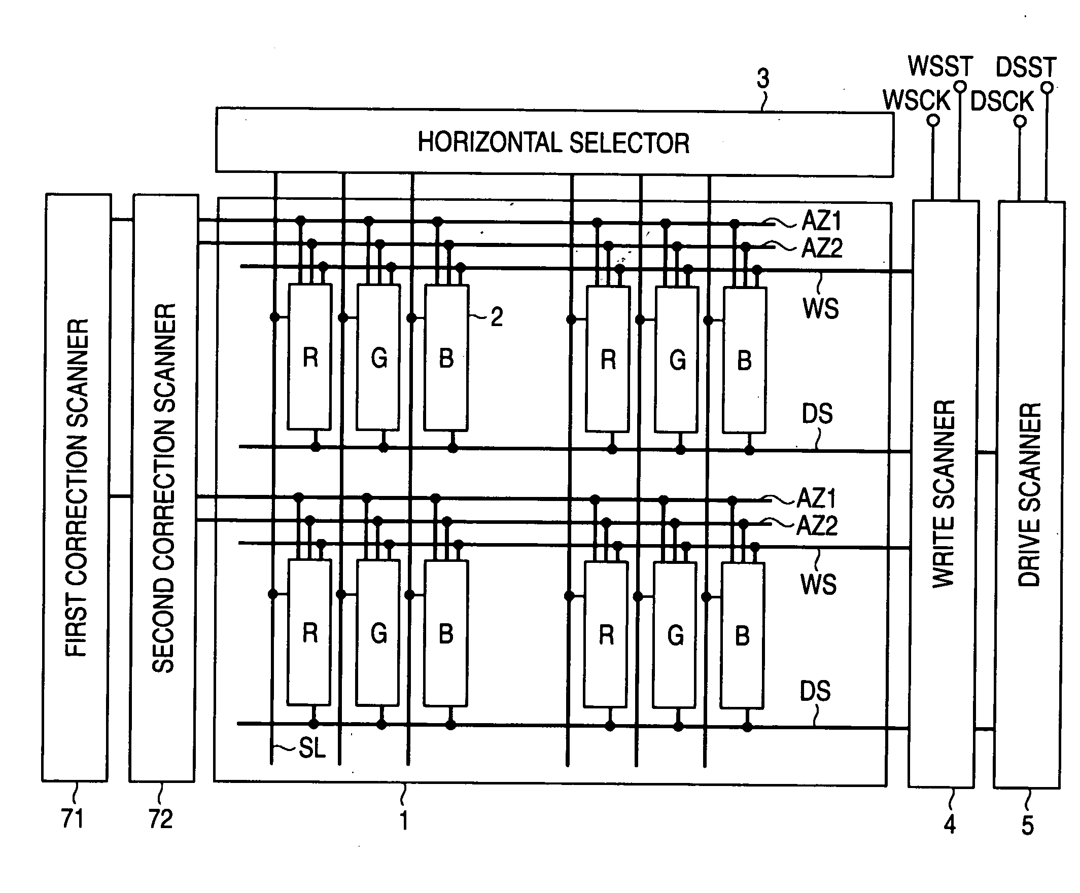
[0076]In the current flat panel market, products with higher screen brightness are in demand. Accordingly, it is necessary to shorten the mobility correction time that acts on the signal potential to be reduced. When the mobility correction time is made shorter, streaks due to uneven brightness are noticeable with a slight shift of duration. The variations in correction time are principally caused by variations in threshold voltages of the switching transistor and the sampling transistor. Accordingly, the basic concept of the invention is to make the transition waveforms of the control signal pulses applied to the gates of these transistors steeper so that, if the threshold voltages of the transistors vary, the correction time itself may not vary. FIG. 10 is a schematic circuit diagram showing the first embodiment created based on the basic concept of the invention. FIG. 10 schematically shows three stages of output units of the write scanner 4 and three columns (three lines) of the...

second embodiment

[0083]FIGS. 13A to 13C are schematic diagrams showing a display device of the second embodiment according to the invention. FIG. 13A shows a pixel configuration, FIG. 13B shows waveforms of control signals WS and DS, and FIG. 13C shows a gate pattern of an output buffer of the write scanner. As shown in FIG. 13A, the embodiment uses a P-channel transistor as the sampling transistor Tr1. Accordingly, as shown in FIG. 13B, the determining waveform of the control signal WS applied to the sampling transistor Tr1 is not the falling waveform shown in FIG. 12, but a rising waveform. Therefore, as shown in FIG. 13C, in the output buffer of the write scanner that supplies the control signal WS, the P-channel transistor is a superior switching element that principally forms the rising waveform of the control signal WS, and the N-channel transistor is an inferior switching element on the contrary. In the embodiment, in order to make the determining waveform steeper, the channel width of the P-...

third embodiment

[0084]FIGS. 14A to 14C are schematic diagrams showing a display device of the third embodiment according to the invention. As shown in FIG. 14A, the embodiment uses an N-channel transistor as the switching transistor Tr4. Accordingly, as shown in FIG. 14B, the rising waveform of the control signal DS is the determining waveform that determines the start of the mobility correction time. As shown in FIG. 14C, in the output buffer of the drive scanner 5 that supplies the control signal DS, the channel width of the P-channel transistor at the superior switching element side that forms the determining waveform is made wider than the channel width of the N-channel transistor at the inferior switching element side. Thereby, the rising waveform of the control signal DS can be made steeper than the falling waveform.


PUM


Abstract

A display device is disclosed. The display device includes: a pixel array part; and a drive part that drives the pixel array part. The pixel array part includes row-wise first scan lines and second scan lines, column-wise signal lines, pixels arranged in a matrix form on parts where the lines intersect, and power supply lines and ground lines that supply power to the respective pixels. The drive part includes a first scanner that sequentially supplies first control signals to the respective first scan lines and line-sequentially scans the pixels in units of rows, a second scanner that sequentially supplies second control signals to the respective second scan lines according to the line-sequential scan, and a signal selector that supplies video signals to the column-wise signal lines according to the line-sequential scan.

Description

CROSS REFERENCES TO RELATED APPLICATIONS[0001]The present invention contains subject matter related to Japanese Patent Application JP 2006-222146 filed in the Japanese Patent Office on Aug. 17, 2006, the entire contents of which being incorporated herein by reference.BACKGROUND OF THE INVENTION[0002]1. Field of the Invention[0003]The present invention relates to a display device that displays images by current-driving light emitting devices provided with respect to each pixel. Specifically, the invention relates to a so-called active matrix type-display device that controls amounts of current to be applied to light emitting devices such as organic EL devices with insulated gate field effect transistors provided within the respective pixel circuits. Further, the invention relates to electronic equipment in which such a display device is incorporated.[0004]2. Background Art[0005]In a display device such as a liquid crystal display, many liquid crystal pixels are arranged in a matrix f...

Claims


Application Information

Patent Timeline
Patent Type & Authority Applications(United States)
IPC IPC(8): G09G3/32H05B44/00
CPCG09G3/3233G09G3/3266G09G2300/0426G09G2300/0439G09G2300/0819G09G2320/043G09G2300/0866G09G2310/0262G09G2310/0289G09G2320/0223G09G2300/0861
Inventor YAMASHITA, JUNICHIUCHINO, KATSUHIDE
Owner JOLED INC
Why Eureka
Try Eureka