A design method and debugging method for mobile phone JTAG debugging interface signals

A debugging interface and design method technology, applied in the direction of telephone communication, sub-office equipment, telephone structure, etc., can solve the problems of design difficulties, safety performance cannot be guaranteed, etc., and meet the needs of convenient application, safe use, and reduced number of signals Effect

Inactive Publication Date: 2008-01-09
ZTE CORP
View PDF0 Cites 12 Cited by
  • Summary
  • Abstract
  • Description
  • Claims
  • Application Information

AI Technical Summary

Problems solved by technology

As mobile phones are now developing towards miniaturization and interface simplification, many mobile phone tail plug signals are facing cancellation or multiplexing. Since JTAG signals involve the control and access of the core of each part of the baseband chip, it is multiplexed with other signals. Can create design difficulties and lead to safety performance not being guaranteed

Method used


Image

  • A design method and debugging method for mobile phone JTAG debugging interface signals
  • A design method and debugging method for mobile phone JTAG debugging interface signals
  • A design method and debugging method for mobile phone JTAG debugging interface signals

Examples


Embodiment Construction

[0030] Preferred embodiments of the present invention are described in detail below.

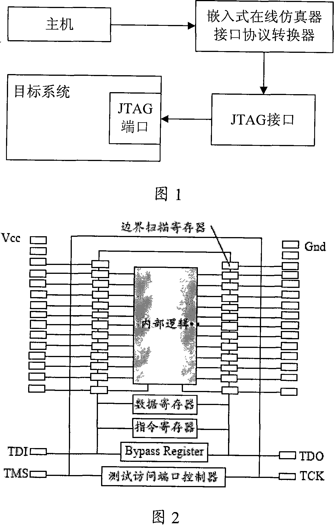
[0031] The invention provides a method for designing a mobile phone JTAG debugging interface signal, wherein: only a clock signal, a conversion signal, a data input signal and a data output signal are set; and a diode is multiplexed with a system reset signal as a core reset signal.

[0032] Specifically, according to the definition of the JTAG protocol (IEEE standard 1149.1), each signal is analyzed as follows:

[0033] 1. JTMS, JTDI, JTDO, JTCK signals are all necessary;

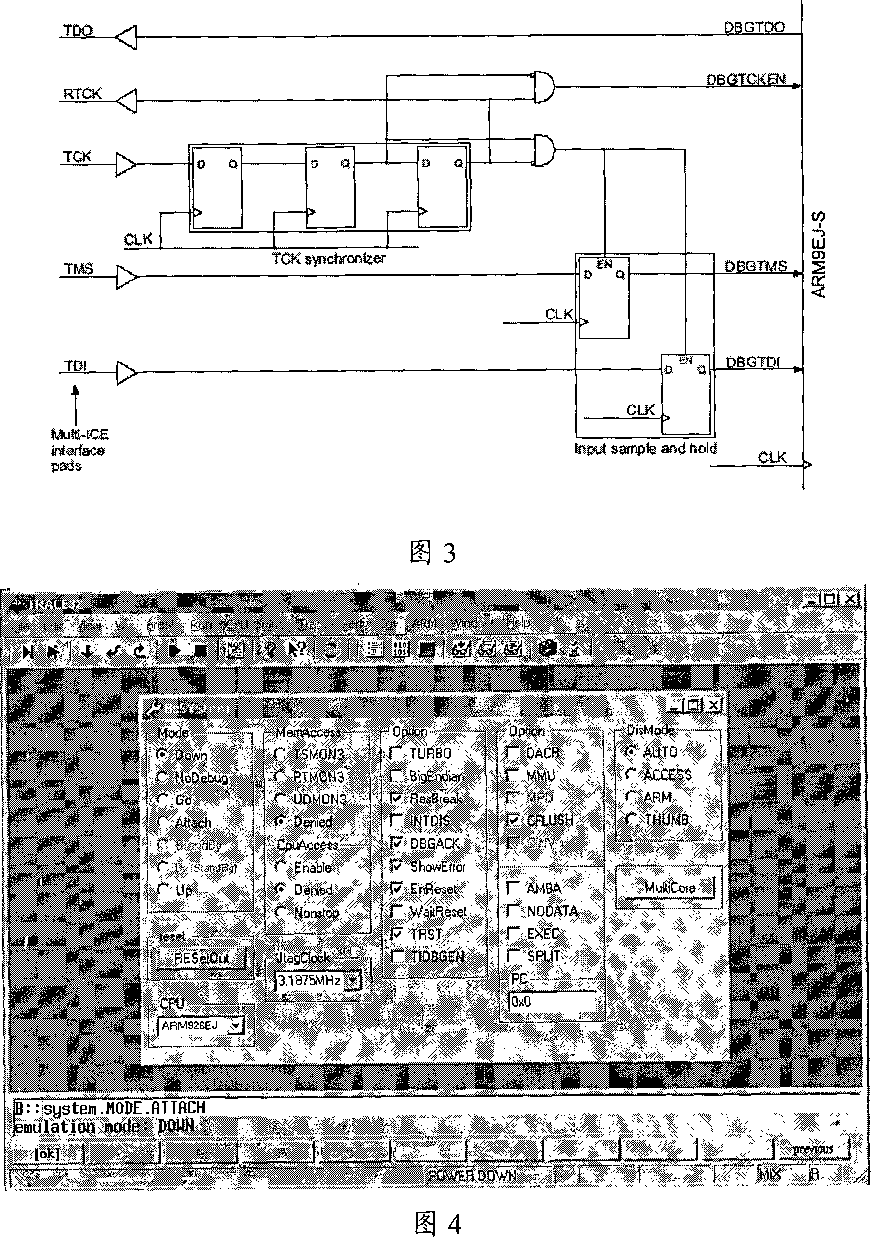
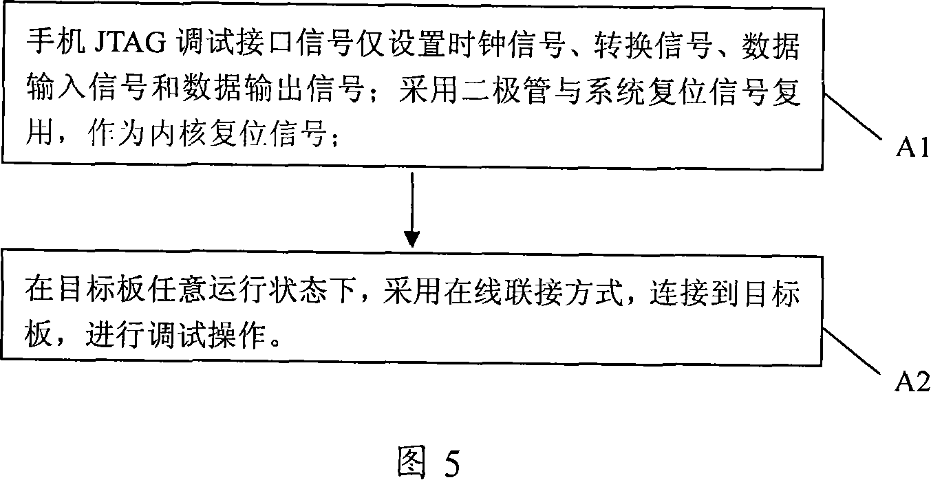
[0034] 2. The JRST signal is used to reset the kernel. In a normal design, the reset signal of the kernel will generally be processed accordingly. This signal is only for when JTAG is connected to the target board, as shown in Figure 4. When the user clicks on the TRACE32 interface When "Target Reset", reset the kernel. Therefore, this signal can be multiplexed with the system reset signal through a diode; under normal...


PUM


Abstract

The method comprises: only setting the clock signal, switch signal, data input signal and data output signal; using the diode and the system reset signal multiplex as inner core reset signal. When the target board runs at any states, a on-line connection approach is used to connect to the target board in order to make a debug operation. The invention realizes the JTAG interface having only four signals so as to simplify the design of JTAC.

Description

technical field [0001] The invention relates to a mobile phone JTAG debugging interface signal, in particular to a method for designing a mobile phone JTAG debugging interface signal and a debugging method thereof. Background technique [0002] JTAG (Joint Test Action Group, Joint Test Action Group) is an international standard test protocol (IEEE 1149.1 compatible), mainly used for chip internal testing. Most of the advanced devices now support the JTAG protocol, such as DSP, FPGA devices and so on. The standard JTAG interface is 4 lines, which are mode selection, clock, data input and data output lines. [0003] The microcontroller of the target system is connected to the emulator or debugging tool through the JTAG interface, and then connected to the relevant port of the PC for debugging. As shown in Figure 1, the host is connected to the embedded ICE (In Circuit Emulator, online emulator) interface protocol converter (that is, the TRACE32 emulator) through the RS232 pr...

Claims


Application Information

Patent Timeline
Patent Type & Authority Applications(China)
IPC IPC(8): H04Q7/32H04Q7/34H04B1/38H04M1/24H04M1/02
Inventor 陈岩侯方西
Owner ZTE CORP
Why Eureka
Try Eureka