Solid-state imaging device, method of manufacturing the same, and electronic apparatus

a solid-state imaging and imaging method technology, applied in the direction of radio frequency controlled devices, instruments, transistors, etc., can solve the problems of increasing the electric field intensity of the p-n junction portion, difficult to obtain a sufficient saturation characteristic, and inability to obtain a sufficient area for the photodiodes, so as to reduce the width of the first isolation region, increase the area of the photodiode, and achieve the effect of sufficient isolation

Active Publication Date: 2013-12-10
SONY CORP
View PDF8 Cites 13 Cited by
  • Summary
  • Abstract
  • Description
  • Claims
  • Application Information

AI Technical Summary

Benefits of technology

[0009]Therefore, when the isolation region is formed of the p-type semiconductor layer having a high concentration, the influence of the diffusion of the p-type impurities of the isolation region toward the photodiode results in an effective area of the photodiode being reduced and the saturation signal amount Qs being reduced. In addition, in the floating diffusion (FD) region, the floating diffusion region having a high concentration adjoins the isolation region having a high concentration so that a high concentration p-n junction is formed. Therefore, the electric field intensity of the p-n junction portion increases, and the white spots in the floating diffusion region worsen. When the electric field is strong and there is a crystal defect, the crystal defect growth rate accelerates, and it is easier for electrons to escape even from a deep level, so that the white spots worsen.
[0023]In the electronic apparatus according to an embodiment of the present invention, it is possible to at least improve pixel characteristics such as a saturation characteristic, sensitivity, and mixed color of the solid-state imaging device by providing the solid-state imaging device as described above. Therefore, it is possible to provide a high-quality electronic apparatus having an improved image quality.

Problems solved by technology

Therefore, it may not be possible to obtain a sufficient area for the photodiodes, and it is difficult to obtain a sufficient saturation characteristic (saturation charge amount Qs).
Therefore, the electric field intensity of the p-n junction portion increases, and the white spots in the floating diffusion region worsen.
In addition, in the case where the element isolation structure is changed within the layout of the pixel portion in consideration of imaging characteristics such as random noise reduction, an optimal impurity concentration is not obtained for each element isolation structure, and this incurs losses in a saturation characteristic, sensitivity, and mixed color.
In the case where ions are collectively implanted, although the isolation concentration can be reduced in the isolation region having the STI structure, optimization is not obtained because a high concentration implantation is to be performed.

Method used


Image

  • Solid-state imaging device, method of manufacturing the same, and electronic apparatus
  • Solid-state imaging device, method of manufacturing the same, and electronic apparatus
  • Solid-state imaging device, method of manufacturing the same, and electronic apparatus

Examples


first embodiment

2. First Embodiment

Exemplary Structure of Solid-State Imaging Device

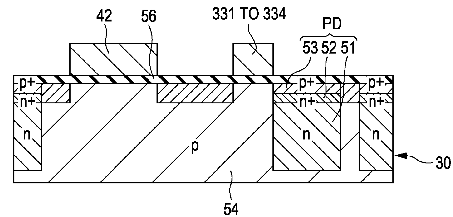
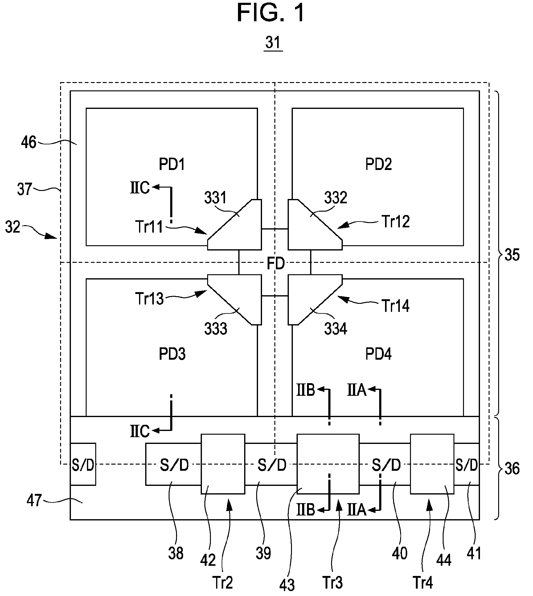
[0079]FIGS. 1 and 2C illustrate a solid-state imaging device according to first embodiment of the present invention. In the present embodiment, a CMOS solid-state imaging device may be applied in which a so-called 4-pixel sharing unit, where 2 horizontal pixels×2 vertical pixels constitute a unit, is arranged in two dimensions. As shown in FIG. 1, in the solid-state imaging device 31 according to the first embodiment of the invention, a pixel portion is constructed by arranging the 4-pixel sharing unit 32 in two dimensions, and the 4-pixel sharing unit 32 is obtained by arranging four photodiodes PD [PD1 to PD4] which are the photoelectric conversion portions of four pixels. The 4-pixel sharing unit 32 share four photodiodes PD and a single pixel transistor group other than the transfer transistors. Specifically, in the 4-pixel sharing unit 32, a single floating diffusion region FD is shared by four photodiodes PD1 ...

second embodiment

3. Second Embodiment

Exemplary Structure of Solid-State Imaging Device

[0113]FIG. 7 illustrates the solid-state imaging device according to the second embodiment of the present invention. In the present embodiment, as described above, a CMOS solid-state imaging device may be applied in which a so-called 4-pixel sharing unit, where 2 horizontal pixels×2 vertical pixels constitute a unit, is arranged in two dimensions. As shown in FIG. 7, in the solid-state imaging device 61 according to the second embodiment of the invention, a pixel portion is constructed by arranging the 4-pixel sharing unit 32 in two dimensions, and the 4-pixel sharing unit 32 is obtained by arranging four photodiodes PD [PD1 to PD4] which are the photoelectric conversion portions of four pixels. As described above, the 4-pixel sharing unit 32 includes the photodiode formation area 35 and the pixel transistor formation area 36, and the first and second isolation regions 46 and 47 are formed from the p-type impurity ...

third embodiment

4. Third Embodiment

Exemplary Structure of Solid-State Imaging Device

[0121]FIG. 8 illustrates a solid-state imaging device according to a third embodiment of the present invention. In the present embodiment, as described above, a CMOS solid-state imaging device may be applied in which a so-called 4-pixel sharing unit, where 2 horizontal pixels×2 vertical pixels constitute a unit, is arranged in two dimensions. As shown in FIG. 8, in the solid-state imaging device 63 according to the third embodiment of the invention, a pixel portion is constructed by arranging the 4-pixel sharing unit 32 in two dimensions, and the 4-pixel sharing unit 32 is obtained by arranging four photodiodes PD [PD1 to PD4] which are the photoelectric conversion portions of four pixels. As described above, the 4-pixel sharing unit 32 includes the photodiode formation area 35 and the pixel transistor formation area 36, and the first and second isolation regions 46 and 47 are formed from the p-type impurity semicon...


PUM


Abstract

A solid-state imaging device includes: a pixel having a photodiode and a pixel transistor; a first isolation region using a semiconductor region containing impurities formed between neighboring photodiodes; and a second isolation region using an semiconductor region containing impurities formed between the photodiode and the pixel transistor, wherein an impurity concentration of the first isolation region is different from an impurity concentration of the second isolation region.

Description

BACKGROUND OF THE INVENTION[0001]1. Field of the Invention[0002]The present invention relates to a solid-state imaging device, a method of manufacturing the same, and an electronic apparatus where the solid-state imaging device is applied to a camera or the like.[0003]2. Description of the Related Art[0004]As a solid-state imaging device, a CMOS solid-state imaging device, a CCD solid-state imaging device, or the like are used. Particularly, since the CMOS solid-state imaging device has a low power source voltage and low power consumption, it is employed in a digital still camera, a digital video camera, and various mobile terminal devices such as a mobile phone with a built-in camera.[0005]For example, the CMOS solid-state imaging device includes a pixel portion where photodiodes which are a photoelectric conversion portion and a plurality of pixels having a plurality of pixel transistors are regularly arranged in two dimensions and a peripheral circuit portion disposed around the ...

Claims


Application Information

Patent Timeline
Patent Type & Authority Patents(United States)
IPC IPC(8): H01L31/00H01L27/146
CPCH01L27/14603H01L27/14609H01L27/14641H01L27/14689H01L27/1463H01L27/14612H01L27/14643
Inventor YANAGITA, TAKESHIKOGA, FUMIHIKOWAKANO, TOSHIFUMINAGANO, TAKASHI
Owner SONY CORP
Why Eureka
Try Eureka