Method for etching grooves

A technology of grooves and etching stop layers, which is applied in the field of semiconductor manufacturing, can solve the problems of reducing the electrical performance of devices, and achieve the effect of narrowing line width and reducing the size of etching

Active Publication Date: 2013-09-18
SEMICON MFG INT (SHANGHAI) CORP
View PDF7 Cites 11 Cited by
  • Summary
  • Abstract
  • Description
  • Claims
  • Application Information

AI Technical Summary

Problems solved by technology

A slight deviation in the line width will change the parameters such as the width, length and resistance of the gate electrode in the produced semiconductor device, which in turn will reduce the electrical performance of the device

Method used


Image

  • Method for etching grooves
  • Method for etching grooves
  • Method for etching grooves

Examples


Embodiment Construction

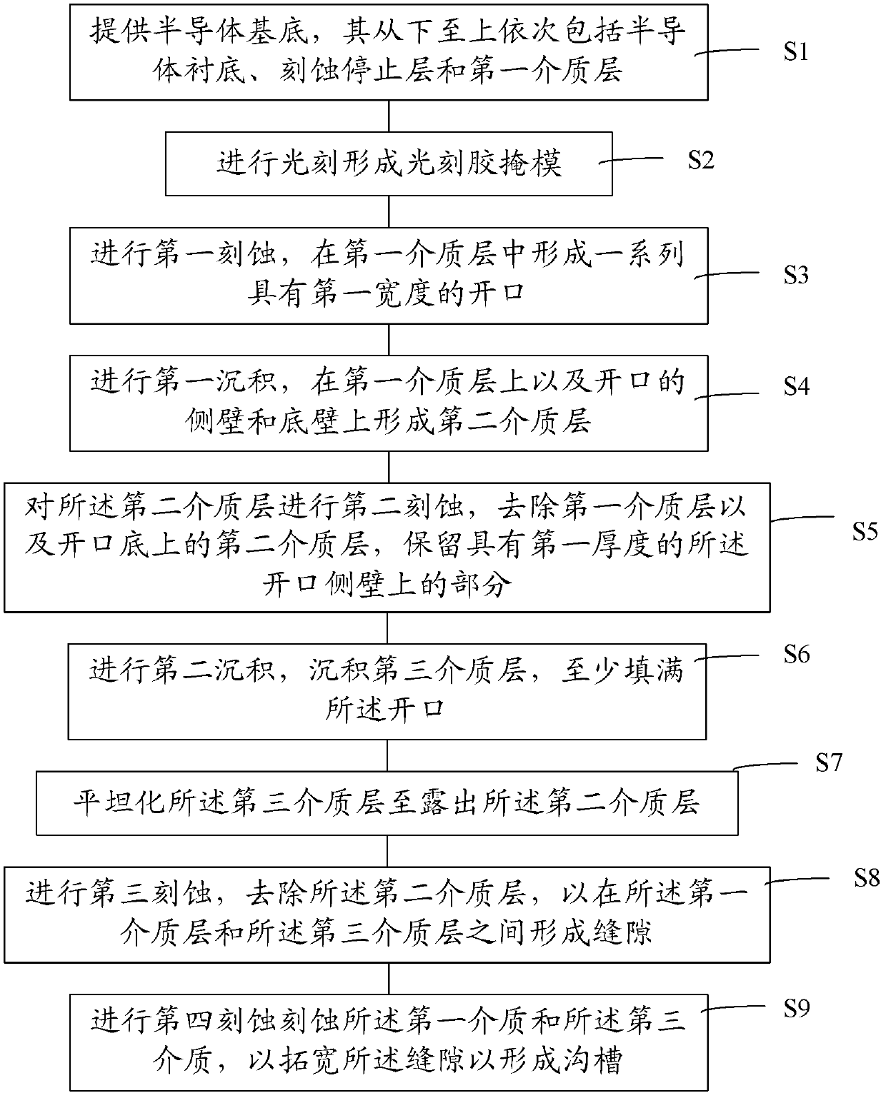
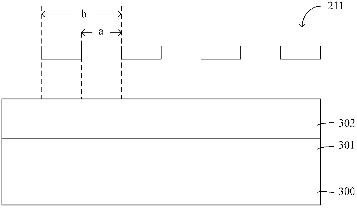
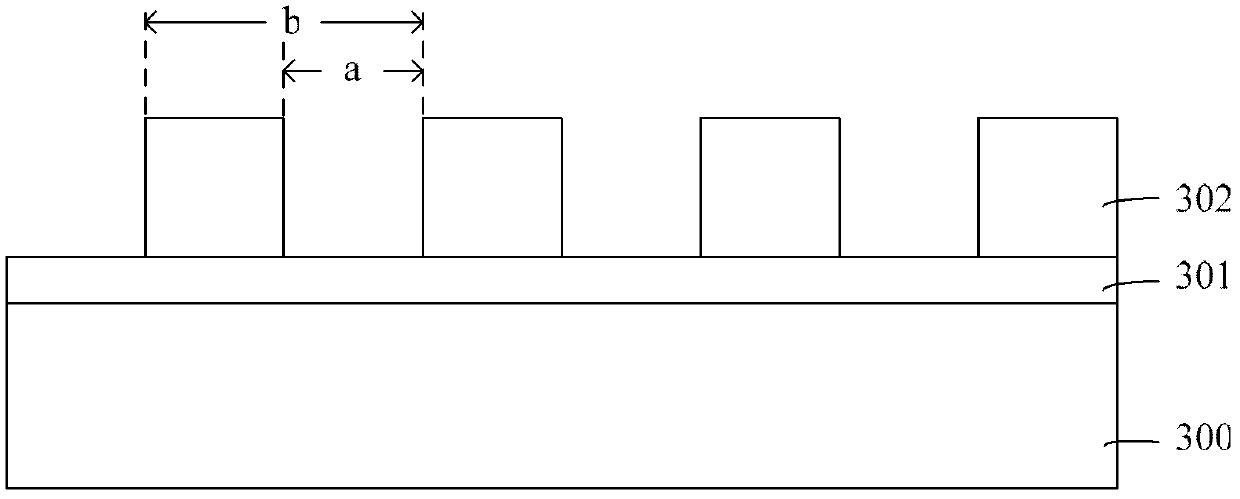
[0033] The present invention only utilizes one photolithography, and then combines the effects of four etchings, so that the width of the opening formed by etching can be only half of the minimum width that can be achieved by photolithography precision, and avoids the need for two Difficulties in overlay accuracy caused by secondary lithography. In this way, the size of the formed trench can be reduced to a large extent while the existing exposure accuracy of the exposure equipment is maintained, so as to adapt to the ever-shrinking line width of the integrated circuit chip. For example, the maximum exposure precision that the existing exposure equipment can generally achieve is 90nm, while the existing advanced integrated circuit process node is 18-23nm. By using the method of the invention, it is easier to use the existing exposure equipment to achieve more advanced process size requirements. The etching method of the present invention mainly comprises four etchings:

[00...


PUM


Abstract

A method for etching grooves comprises: providing a semiconductor substrate on which an etching stop layer and a first dielectric layer are formed in sequence; forming a photoresist mask; performing a first etching so that openings, each of which is with a first width, are formed on the first dielectric layer; performing a first depositing and thus a second dielectric layer is formed; performing a second etching on the second dielectric layer and removing the second dielectric layer that is on the first dielectric layer and the bottom walls of the openings so that the second dielectric layer that is on the side walls of the openings, each of which is with the first width, is remained; performing a second depositing and depositing a third dielectric layer so that the third dielectric layer at least fills up the openings; flattening the third dielectric layer until the second dielectric layer is exposed; performing a third etching to remove the second dielectric layer so that gaps are formed between the first dielectric layer and the third dielectric layer; and performing a fourth etching to etch the first dielectric layer and the third dielectric layer so that the gas are widened to form grooves. According to the method, a more advanced process dimension requirement can be realized with current exposure equipment.

Description

technical field [0001] The invention relates to the field of semiconductor manufacturing, in particular to a groove etching method in the field of double pattern technology. Background technique [0002] In order to integrate more and smaller transistors on a chip, new photolithography techniques must be developed to continuously reduce the size of transistors. [0003] One direction of development in lithography is to fundamentally shorten the wavelength of light used in optical lithography. The current lithography technology is devoted to the development of extreme ultraviolet (EUV) lithography technology with a wavelength of 13.5 nm. Using EUV lithography technology may result in chips with feature sizes smaller than 32nm. Chips using EUV lithography will end up being 100 times faster and have 100 times more storage than even the most processing-capable chips available today. However, there are still many problems in the current EUV lithography technology that have not...

Claims


Application Information

Patent Timeline
Patent Type & Authority Applications(China)
IPC IPC(8): H01L21/02H01L21/311
Inventor 何其旸
Owner SEMICON MFG INT (SHANGHAI) CORP
Why Eureka
Try Eureka