Chip trench preparing method and chip preparing method

A groove and chip technology, which is applied in semiconductor/solid-state device manufacturing, electrical components, circuits, etc., can solve the problems of exposure and development precision limitations and the inability to reduce the size of grooves, etc.

Inactive Publication Date: 2020-02-11
GREE ELECTRIC APPLIANCES INC
View PDF5 Cites 0 Cited by
  • Summary
  • Abstract
  • Description
  • Claims
  • Application Information

AI Technical Summary

Problems solved by technology

[0003] The first object of the present invention is to provide a method for preparing chip grooves, so as to solve the problem in the prior art that the...

Method used


Image

  • Chip trench preparing method and chip preparing method
  • Chip trench preparing method and chip preparing method
  • Chip trench preparing method and chip preparing method

Examples


Embodiment Construction

[0031] In order to make the purpose, technical solutions and advantages of the embodiments of the present invention clearer, the technical solutions in the embodiments of the present invention will be clearly and completely described below in conjunction with the drawings in the embodiments of the present invention. Obviously, the described embodiments It is a part of embodiments of the present invention, but not all embodiments. Based on the embodiments of the present invention, all other embodiments obtained by persons of ordinary skill in the art without making creative efforts belong to the protection scope of the present invention.

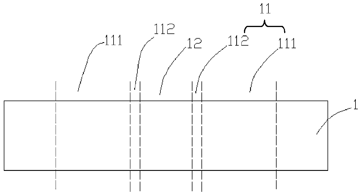
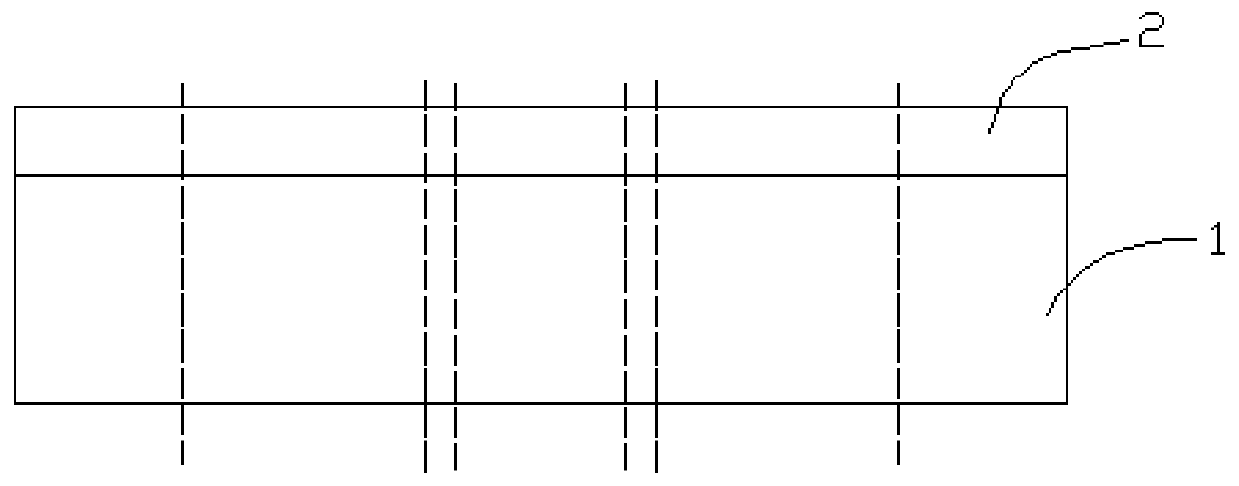
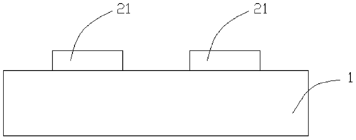
[0032] In a first aspect, the present invention provides a method for preparing chip trench 5, referring to Figure 1-Figure 6 ,include:

[0033] A substrate 1 is provided, and a trench region 12 and a non-trench region 11 surrounding the trench region 12 are preset on the surface of the substrate 1; wherein, the non-trench region 11 includes...


PUM


Abstract

The invention relates to a method for preparing a chip trench and a method for preparing a chip. The method for preparing a chip trench includes: providing a substrate; presetting a trench region on asurface of the substrate; A non-groove region; wherein the non-groove region includes a preset barrier region and a transition region, the transition region surrounding the trench region, and the barrier region surrounding the transition region; corresponding to the barrier region A mask is formed on the surface of the substrate; a side wall is formed on the surface of the substrate correspondingto the transition region and on the sidewall of the mask, and the side wall forms a Etch holes; etch the substrate at the etch holes to form trenches. The preparation method of the present inventioncan solve the problem that the size of the trench cannot be reduced due to the limitation of the accuracy of exposure and development when the trench is prepared by the photolithography technology inthe prior art, and the purpose of reducing the size of the trench is achieved.

Description

technical field [0001] The invention relates to the technical field of semiconductors, in particular to a method for preparing a chip groove and a method for preparing a chip. Background technique [0002] Reducing the chip area is a common goal in the current chip research and development field. In order to improve various performance indicators of the chip, it is often necessary to prepare grooves on the substrate. However, as the chip area continues to decrease, the size of the grooves prepared correspondingly also decreases. Due to the limitation of photolithography technology, if the groove size is too small, the precision of exposure and development is not enough, and there is a large error. Therefore, it is not feasible to use the current method of directly using the photomask to reduce the size of the trench. Contents of the invention [0003] The first object of the present invention is to provide a method for preparing chip grooves, so as to solve the problem i...

Claims


Application Information

Patent Timeline
IPC IPC(8): H01L21/308
CPCH01L21/3081H01L21/3086
Inventor 王文兵史波肖婷
Owner GREE ELECTRIC APPLIANCES INC
Why Eureka
Try Eureka