Semiconductor device and manufacturing method thereof

A device manufacturing method and semiconductor technology, applied in semiconductor/solid-state device manufacturing, semiconductor devices, transistors, etc., can solve the problems of difficult small-sized device threshold adjustment, process instability, etc., and achieve the effect of improving device performance

Active Publication Date: 2013-09-18
INST OF MICROELECTRONICS CHINESE ACAD OF SCI
View PDF5 Cites 39 Cited by
  • Summary
  • Abstract
  • Description
  • Claims
  • Application Information

AI Technical Summary

Problems solved by technology

[0007] However, this method of adjusting the work function only by controlling the film thickness ratio is no longer suitable for ultra-thin and ultra-small devices due to the large process instability after the film thickness reaches the nanometer level, so it is difficult to rationally optimize the control Threshold Adjustment for Small Devices

Method used


Image

  • Semiconductor device and manufacturing method thereof
  • Semiconductor device and manufacturing method thereof
  • Semiconductor device and manufacturing method thereof

Examples


Embodiment Construction

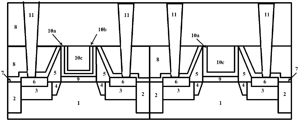
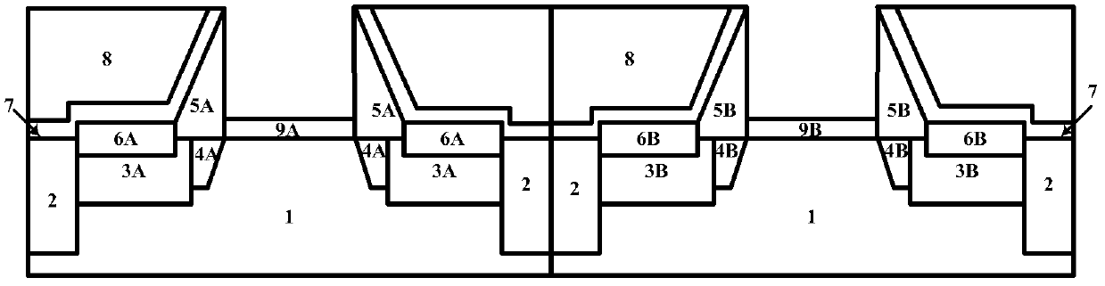
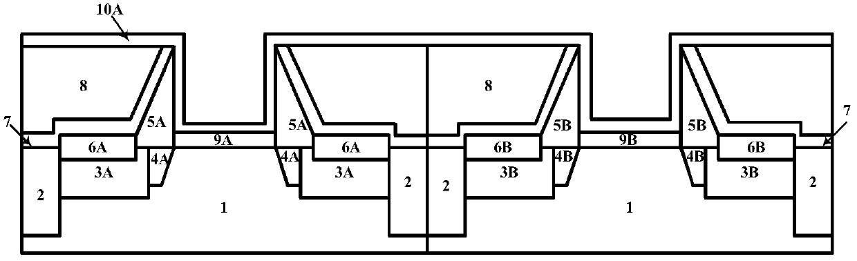
[0035] The features and technical effects of the technical solution of the present invention will be described in detail below with reference to the accompanying drawings and in combination with schematic embodiments, and a novel MOSFET capable of effectively adjusting the work function of the metal gate to control the threshold and its manufacturing method are disclosed. It should be pointed out that similar reference numerals represent similar structures, and the terms "first", "second", "upper", "lower" and the like used in this application can be used to modify various device structures or manufacturing processes . These modifications do not imply spatial, sequential or hierarchical relationships of the modified device structures or fabrication processes unless specifically stated.

[0036] The following will refer to Figure 2 to Figure 10 A cross-sectional schematic diagram is used to illustrate each step of the CMOSFET manufacturing method according to the present inve...


PUM


Abstract

The invention discloses a semiconductor device, which comprises a substrate, a plurality of gate stacking structures on the substrate, a plurality of gate side wall structures on the two sides of each gate stacking structure, and a plurality of source-drain regions in the substrate on the two sides of each gate side wall structure. The gate stacking structures comprise a plurality of first gate stacking structures and a plurality of second gate stacking structures, wherein each first gate stacking structure comprises a first gate insulating layer, a first work function metal layer, a second work function metal diffusion barrier layer and a gate filling layer, and the work function is close to a valance band (conduction band) side. Each second gate stacking structure comprises a second gate insulating layer, a modified first work function metal layer, a second work function metal layer and a gate filling layer. The semiconductor device is characterized in that the second work function metal layer comprises injected doping ions for adjusting the work function, and part of the first work function layer which is diffused below the second work function mental layer is used for adjusting a threshold to enable the work function of a gate to be close to the conduction band (valence band) side and to correspond to a first work function, so that the work function of the gate is accurately adjusted.

Description

technical field [0001] The invention relates to a semiconductor device and a manufacturing method thereof, in particular to a MOSFET and a manufacturing method thereof which use metal injection to adjust work function. Background technique [0002] Starting from the 45nm CMOS integrated circuit process, with the continuous reduction of device feature size, in order to suppress the short channel effect, the equivalent oxide thickness (EOT) of the gate insulating dielectric layer in CMOS devices must be reduced simultaneously. However, due to the low (relative) dielectric constant (for example, about 3.9) of the ultra-thin (eg 10nm) conventional oxide layer or oxynitride layer, the insulation performance is difficult to withstand the relatively high field strength in such ultra-small devices, which will cause serious damage. gate leakage. Therefore, the traditional polysilicon (poly-si) / SiON system is no longer applicable. [0003] In view of this, the industry has begun to ...

Claims


Application Information

Patent Timeline
Patent Type & Authority Applications(China)
IPC IPC(8): H01L27/092H01L21/8238
CPCH01L21/823842H01L21/823857H01L29/4966H01L29/518H01L29/66545H01L29/66606H01L29/7833
Inventor 殷华湘徐秋霞赵超陈大鹏
Owner INST OF MICROELECTRONICS CHINESE ACAD OF SCI
Why Eureka
Try Eureka