Strained superlattice tunnel junction ultraviolet led epitaxial structure and its preparation method

An epitaxial structure and superlattice technology, applied in electrical components, circuits, semiconductor devices, etc., can solve problems such as ohmic contact bottlenecks, and achieve the effect of reducing resistivity, improving current expansion performance, and enhancing performance

Active Publication Date: 2016-01-20
XI AN JIAOTONG UNIV
View PDF4 Cites 1 Cited by
  • Summary
  • Abstract
  • Description
  • Claims
  • Application Information

AI Technical Summary

Problems solved by technology

[0008] The technical problem to be solved by the present invention is to provide a tunnel junction ultraviolet LED epitaxial structure and preparation method to increase the hole carrier concentration of the p-type AlGaN layer and solve the ohmic contact bottleneck problem

Method used


Image

  • Strained superlattice tunnel junction ultraviolet led epitaxial structure and its preparation method
  • Strained superlattice tunnel junction ultraviolet led epitaxial structure and its preparation method
  • Strained superlattice tunnel junction ultraviolet led epitaxial structure and its preparation method

Examples


Embodiment Construction

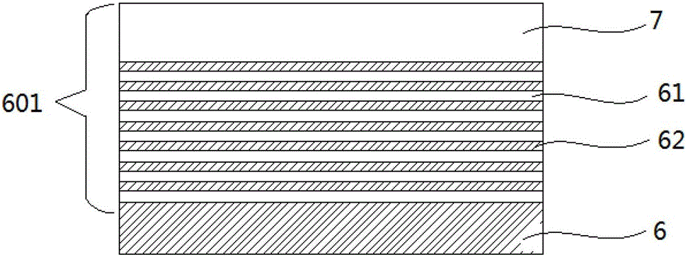
[0030]The invention provides a method for manufacturing a tunnel junction-enhanced ultraviolet LED epitaxial structure, which uses the strain field generated by the superlattice to move the energy band of the AlGaN material in the SSL structure to a low-energy direction as a whole, and forms p-AlGaN / SSL / n*-AlGaN tunnel junction, providing hole carriers. Include at least the following steps:

[0031] Using MOCVD (Metal-organicChemicalVaporDepositiong, metal organic compound chemical vapor deposition) or PAMBE system for epitaxial growth:

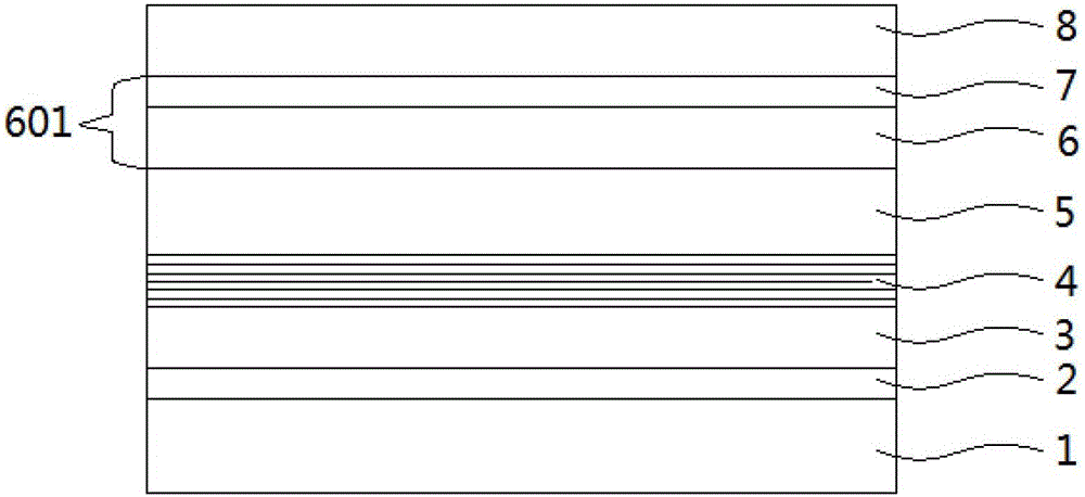
[0032] 1) Prepare an AlN buffer layer 2 on the epitaxial substrate 1, with a thickness of 10 nm to 500 nm;

[0033] 2) growing Si-doped n-type Al on the substrate 1 on which the AlN buffer layer 2 has been grown 0.77 Ga 0.23 N layer;

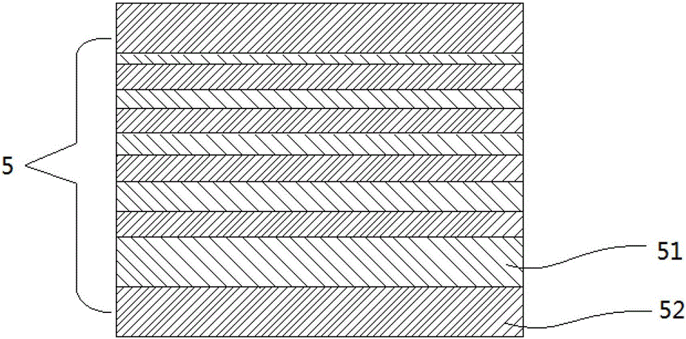
[0034] 3) Five multiple quantum well layers 4 are alternately grown on the n-type AlGaN layer 3; the material of the multiple quantum well layers is Al 0.65 Ga 0.35 N / Al 0.7 Ga 0.3 N;

[0035] 4) Mult...


PUM


Abstract

The invention provides a strained superlattice tunnel junction ultraviolet LED (light emitting diode) epitaxial structure and a production method thereof. The epitaxial structure from top to bottom comprises: an epitaxial growth substrate, an AlN buffer layer, an n-type AlGaN layer, a multiple quantum wells, an electron blocking layer, a strained superlattice, an n-type degenerate doped AlGaN layer, and an n-type Si-doped AlGaN layer. The strained superlattice comprises a p-type AlGaN layer and an AlyGa1-yN / AlxGa1-xN. An AlGaN energy band, under effects of a polarized electric field, moves as a whole along a low energy direction. A superlattice structure contacts a heavily doped n-type AlGaN to form a p-AlGaN / SSL / n *-AlGaN tunnel junction. Electrons of a p-type AlGaN valence band, under effects of an external electric field, carried out tunneling through a tunnel effect to one side of the n-type AlGaN, and a hole is formed in the p-type AlGaN. The n-AlGaN is used as the cladding material instead of the p-type AlGaN, so that the problem of the p-type ohmic contact is avoided.

Description

【Technical field】 [0001] The invention belongs to the technical field of semiconductor light-emitting diodes, and in particular relates to an ultraviolet LED epitaxial structure and a preparation method thereof which utilize a strained superlattice tunnel junction structure to enhance the performance of a p-type nitride material. 【Background technique】 [0002] Ultraviolet light emitting diode (light emitting diode, hereinafter referred to as LED), because of its short wavelength, high photon energy, and uniform beam, has important applications in the fields of physical sterilization, high color rendering index lighting, and high-density optical storage. At present, a large number of researches have made important breakthroughs in crystal quality, high Al composition and short-wavelength structure design, and successfully prepared deep ultraviolet LED devices below 300 nanometers to achieve milliwatt-level power output and reliability. great progress has been made. [0003]...

Claims


Application Information

Patent Timeline
Patent Type & Authority Patents(China)
IPC IPC(8): H01L33/04H01L33/00
Inventor 云峰王越黄亚平田振寰王宏
Owner XI AN JIAOTONG UNIV
Why Eureka
Try Eureka