Supercharge Your Innovation With Domain-Expert AI Agents!

A chip defect detection method

A detection method and technology for chip defects, applied in the direction of semiconductor/solid-state device testing/measurement, etc., can solve the problems of rough detection, inability to accurately perform defect detection, and influence of defect detection accuracy, and achieve the effect of improving the success rate

Active Publication Date: 2016-06-08
SHANGHAI HUALI MICROELECTRONICS CORP
View PDF5 Cites 0 Cited by
  • Summary
  • Abstract
  • Description
  • Claims
  • Application Information

AI Technical Summary

Problems solved by technology

The defect detection method disclosed in this patent needs to provide a master substrate and detect the substrate to be inspected based on the master substrate. The implementation of this method needs to rely on an additional master substrate. If damage occurs, it will affect the accuracy of defect detection; moreover, it divides the adjacent die into multiple regions, and detects defects by using the regions as units. Therefore, this detection method only Can roughly detect defects in integrated circuit products, but cannot accurately detect defects
[0010] It can be seen that there is no detection method with high feasibility and high detection accuracy in the existing defect detection methods.

Method used


Image

  • A chip defect detection method
  • A chip defect detection method
  • A chip defect detection method

Examples


Embodiment 1

[0055] First, the position of the wafer with multiple identical chips prepared on the surface is fixed. The multiple identical chips are arranged in a matrix. After the wafer position is fixed, a direction is selected to scan the wafer row by row. The optical detection equipment may preferably adopt high-sensitivity optical detection equipment to perform the progressive scanning, and obtain optical images of all the chips in the entire wafer to be tested by scanning the wafer progressively.

[0056] Then, the obtained optical image is converted into a data image represented by different bright and dark gray scales, so as to be used in the subsequent detection and comparison process.

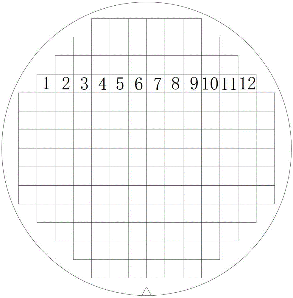
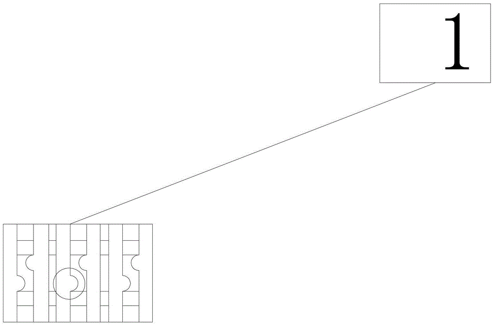
[0057] Such as figure 2 As shown, the chip in the fourth row and the fourth column starting from the top of the wafer is selected as the chip 4 to be tested in the entire wafer, and an appropriate spacing value is selected according to the manufacturing process of the chip to be tested. In this ...

Embodiment 2

[0061] The difference between this embodiment and Embodiment 1 is that when the chip to be tested is selected as Figure 4 As shown in , when it is located at the edge position of the wafer (such as row 4, column 1), at this time, since the chip to be tested is located at the first position in row 4, it is also the first position in column 1 position, at this time, no matter what value the spacing value is set to, the chip to be tested can not find two contrasting chips equal to the spacing of the chip to be tested no matter in the row or the column. Therefore, in this embodiment, it is mainly solved. The detection problem of a class of chips.

[0062] Same as Example 1, firstly, the position of the wafer with multiple identical chips prepared on the surface is fixed, wherein the multiple identical chips are arranged in a matrix, and after the wafer position is fixed, a direction is selected to carry out the process on the wafer. Progressive scanning, wherein an optical detec...


PUM


Abstract

The invention relates to a method for detecting chip defects. The method for detecting the chip defects includes the following steps: S1, offering a wafer, wherein a plurality of identical chips are manufactured on the surface of the wafer, and the chips are arranged on the wafer in a matrix mode; S2, selecting a to-be-tested chip, selecting at least two contrast chips according to the to-be-tested chip, wherein the to-be-tested chip and the contrast chips form a chip set, and the chips in the chip set are arranged on the same straight line at equal intervals; S3, obtaining the data image of the to-be-tested chip and the data images of the contrast chips, and S4, respectively comparing the data images of the contrast chips with the data image of the to-be-tested chip one by one. The to-be-tested chip has defects if an abnormal condition is discovered. The distance between every two adjacent chips in the chip set is N, and N is a positive integer.

Description

technical field [0001] The invention relates to a detection method in the manufacturing process of a semiconductor chip, in particular to a chip defect detection method. Background technique [0002] In recent years, with the rapid development of semiconductor integrated circuits, the performance of integrated circuit devices is also rapidly improving. With the improvement of the performance of integrated circuit devices, the manufacturing process has become more and more complicated. Currently, advanced integrated circuit It contains hundreds of process steps. Therefore, a problem in one of the steps will cause the problem of the entire semiconductor integrated circuit chip. It is manifested that the performance of the semiconductor integrated circuit fails to meet the design requirements, and it may even lead to the failure of the entire chip. [0003] Therefore, in the manufacturing process of semiconductor integrated circuits, it is particularly important to detect the p...

Claims


Application Information

Patent Timeline
Patent Type & Authority Patents(China)
IPC IPC(8): H01L21/66
Inventor 倪棋梁陈宏璘龙吟
Owner SHANGHAI HUALI MICROELECTRONICS CORP
Features
  • R&D
  • Intellectual Property
  • Life Sciences
  • Materials
  • Tech Scout
  • Unparalleled Data Quality
  • Higher Quality Content
  • 60% Fewer Hallucinations
Learn More