Chip defect detection method
A detection method and chip defect technology, which is applied in semiconductor/solid-state device testing/measurement, electrical components, circuits, etc., can solve problems such as low detection accuracy, poor detection rate, and low detection rate, so as to improve selection efficiency, The effect of reducing difficulty and increasing success rate
- Summary
- Abstract
- Description
- Claims
- Application Information
AI Technical Summary
Problems solved by technology
Method used
Image

Examples
Embodiment 1
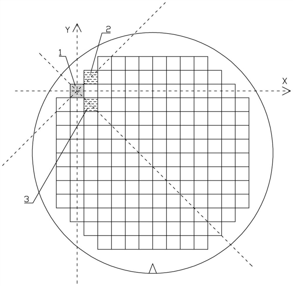
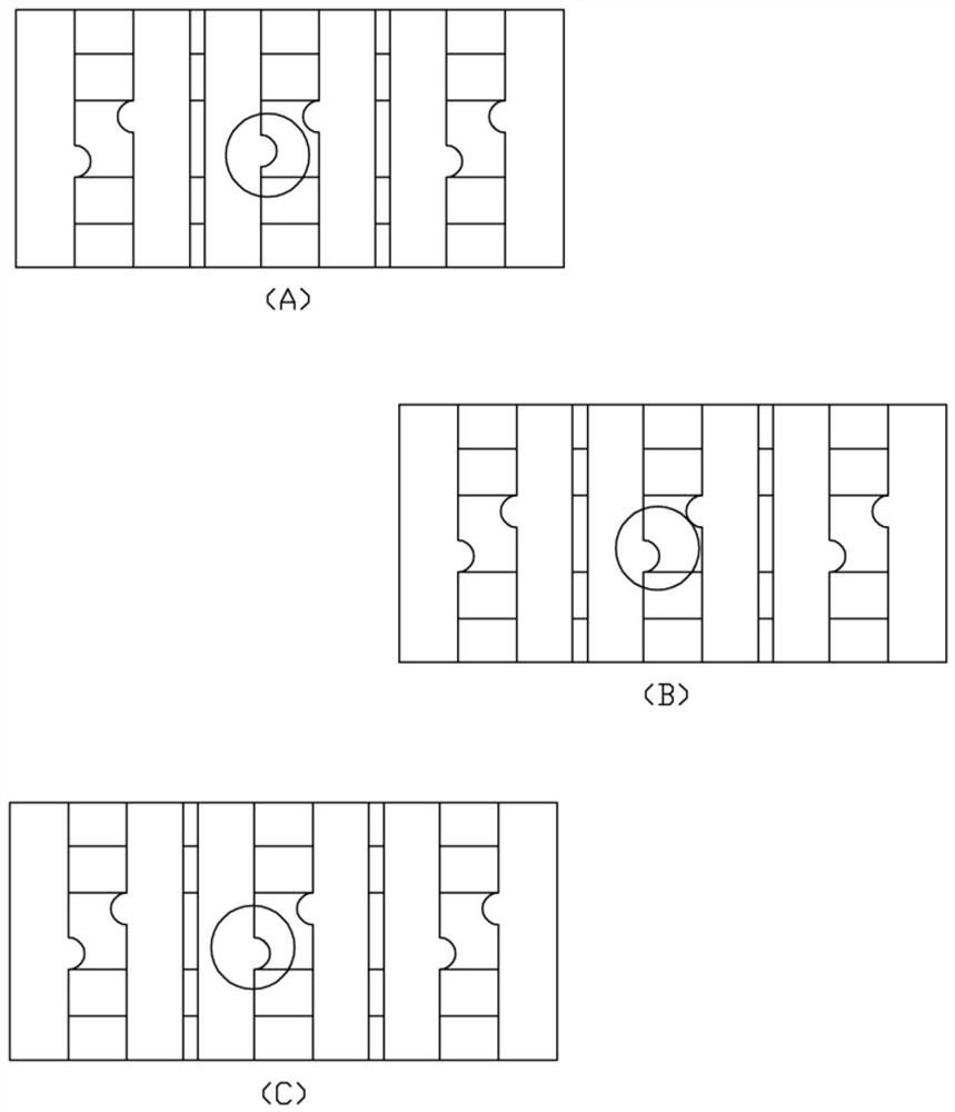
[0042] Such as figure 1 As shown, chip A 1 is selected as the chip to be tested, and the geometric center of chip A 1 is used as the origin as a plane rectangular coordinate system. The X axis of the plane rectangular coordinate system is perpendicular to the opening direction of the wafer alignment mark, and the Y axis is perpendicular to the opening direction of the wafer alignment mark. The opening direction of the wafer alignment mark is parallel, and B chip 2 and C chip 3 on the four quadrant angle bisectors of the plane Cartesian coordinate system are selected as comparison chips; then the wafer is scanned by an optical detection device equipped with high sensitivity, Obtain the optical image of the chip on the wafer, convert the optical image to form a data image, and the data image is represented by different bright and dark gray scales; for example figure 2 A. figure 2 B and figure 2 As shown in C, there is a difference between the data image of A chip 1 and the ...
Embodiment 2
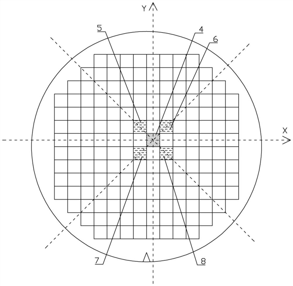
[0044] Such as image 3 As shown, the D chip 4 is selected as the chip to be tested, and the geometric center of the D chip 4 is used as the origin of the plane Cartesian coordinate system. The X axis of the plane Cartesian coordinate system is perpendicular to the opening direction of the wafer alignment mark, and the Y axis is perpendicular to the opening direction of the wafer alignment mark. The opening direction of the wafer alignment mark is parallel, and E chip 5, F chip 6, G chip 7, and H chip 8 on the four quadrant angle bisectors of the plane Cartesian coordinate system are selected as comparison chips; The detection equipment scans the wafer to obtain the optical image of the chip on the wafer, and converts the optical image to form a data image. The data image is represented by different bright and dark gray scales; for example Figure 4 A. Figure 4 B. Figure 4 C. Figure 4 D and Figure 4 As shown in E, there is a difference between the data image of D chip ...
PUM
 Abstract
Description
Claims
Application Information
 - R&D
- Intellectual Property
- Life Sciences
- Materials
- Tech Scout
- Unparalleled Data Quality
- Higher Quality Content
- 60% Fewer Hallucinations
Browse by: Latest US Patents, China's latest patents, Technical Efficacy Thesaurus, Application Domain, Technology Topic, Popular Technical Reports.
© 2025 PatSnap. All rights reserved.Legal|Privacy policy|Modern Slavery Act Transparency Statement|Sitemap|About US| Contact US: help@patsnap.com