SiC junction barrier Schottky diode and manufacturing method thereof

A junction-barrier Schottky and diode technology, applied in semiconductor/solid-state device manufacturing, electrical components, circuits, etc., can solve the problem of limited range of breakdown voltage increase

Active Publication Date: 2013-10-09
TSINGHUA UNIV
View PDF2 Cites 17 Cited by
  • Summary
  • Abstract
  • Description
  • Claims
  • Application Information

AI Technical Summary

Problems solved by technology

It can be considered that the reverse characteristics of the device will still be affected by P + Constrained by the concentrated electric field at the corner of the region, so this structure has a limited range to improve the breakdown voltage

Method used


Image

  • SiC junction barrier Schottky diode and manufacturing method thereof
  • SiC junction barrier Schottky diode and manufacturing method thereof
  • SiC junction barrier Schottky diode and manufacturing method thereof

Examples


Embodiment Construction

[0026] The specific implementation manners of the present invention will be further described in detail below in conjunction with the accompanying drawings and embodiments. The following examples are used to illustrate the present invention, but are not intended to limit the scope of the present invention.

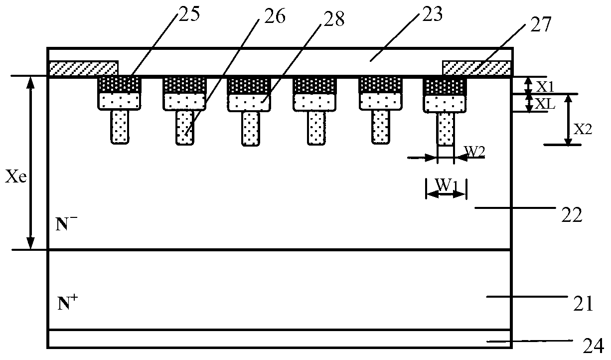
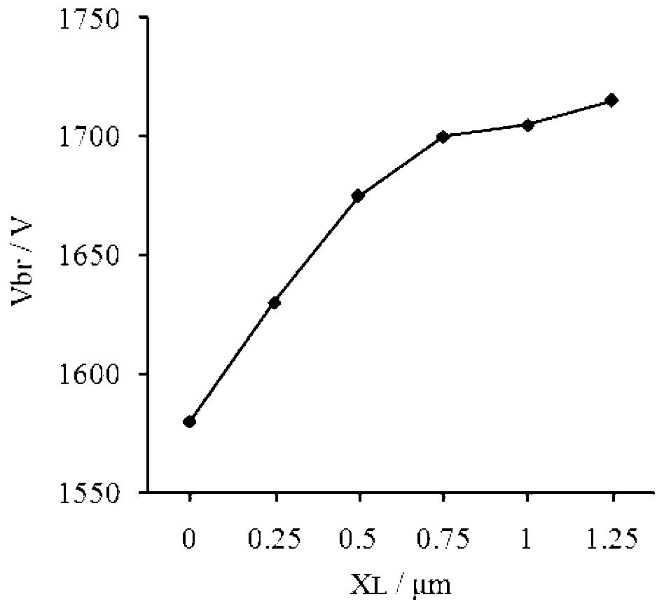
[0027] figure 2 It is a structural cross-sectional view of a SiC junction barrier Schottky diode according to an embodiment of the present invention. like figure 2 shown, with figure 1 The structure of the SiC junction barrier Schottky diode is similar, also with N + Type SiC substrate 21, N - Type SiC epitaxial layer 22 , Schottky metal contact 23 , N-type ohmic contact 24 and insulating layer 27 , the same parts will not be repeated here. Compared with the existing POP type SiC junction barrier Schottky diode, the SiC junction barrier Schottky diode according to the embodiment of the present invention maintains a narrow P - With the well area unchanged, the figu...


PUM


Abstract

The invention relates to a SiC junction barrier Schottky diode and a manufacturing method of the SiC junction barrier Schottky diode. The SiC junction barrier Schottky diode comprises a substrate of a first conductive type, an epitaxial layer of the first conductive type, a Schottky metal contact, a heavily doped region of a second conductive type, a light doped region of the second conductive type, a light doped trap of the second conductive type and an ohmic contact, wherein the epitaxial layer of the first conductive type is formed on the substrate, the Schottky metal contact is formed on the epitaxial layer, the heavily doped region of the second conductive type is formed below the Schottky metal contact, the light doped region of the second conductive type is formed below the heavily doped region, the light doped trap of the second conductive type is formed below the light doped region, the width of the light doped trap is smaller than that of each light doped region, and the ohmic contact is formed on the reverse side of the substrate. The SiC junction barrier Schottky diode can obviously reduce the electric field concentration effect in the corner of a PN junction, and further improves the reverse breakdown voltage of a device and a quality factor (BFOM) value of Baliga.

Description

technical field [0001] The invention relates to the technical field of semiconductor devices, in particular to a SiC junction barrier Schottky diode and a manufacturing method thereof. Background technique [0002] Silicon carbide (SiC) is a typical representative of the third-generation semiconductor materials. Due to the advantages of high thermal conductivity, high saturation drift velocity and high breakdown electric field, SiC materials are especially suitable for extreme environments such as high temperature, high frequency and high radiation. high-power devices in SiC power diodes are an important branch of SiC power devices, mainly including Schottky barrier diodes (SBDs), PIN diodes and junction barrier Schottky diodes (JBS). Among them, the SiC junction barrier Schottky diode combines the advantages of SBD and PIN diodes. It not only has the excellent switching characteristics of SBD, but also has a high blocking ability close to that of PIN diodes. It is expected...

Claims


Application Information

Patent Timeline
Patent Type & Authority Applications(China)
IPC IPC(8): H01L29/872H01L21/329H01L29/06
CPCH01L29/872
Inventor 岳瑞峰信婉清张莉王燕
Owner TSINGHUA UNIV
Why Eureka
Try Eureka