High-power LED chip packaging quality inspection method

A quality inspection method and LED chip technology, which are applied in the direction of single semiconductor device testing, etc., can solve the problems that are not suitable for the inspection of high-power LED chip packaging quality, and are not suitable for online batch inspection of high-power LED packaging quality.

Inactive Publication Date: 2015-08-05
PUTIAN UNIV
View PDF7 Cites 0 Cited by
  • Summary
  • Abstract
  • Description
  • Claims
  • Application Information

AI Technical Summary

Problems solved by technology

Chinese patent application 200710078657.X discloses a non-contact online detection method suitable for small LED chip packaging quality, but not suitable for high-power LED chip packaging quality detection
[0005] In short, the existing LED inspection methods are mainly suitable for LED epitaxial wafer inspection or finished product inspection, and are not suitable for online batch inspection of high-power LED packaging quality

Method used


Image

  • High-power LED chip packaging quality inspection method
  • High-power LED chip packaging quality inspection method
  • High-power LED chip packaging quality inspection method

Examples


Embodiment Construction

[0019] The present invention is described below in conjunction with accompanying drawing.

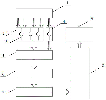
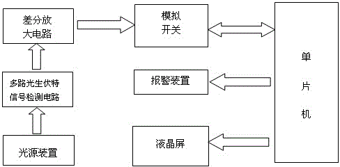
[0020] High-power LED chip packaging quality inspection method, the principle block diagram is as follows figure 1 Shown: During the LED chip packaging process, the uniform light field generated by the light source device (1) is used to vertically irradiate the light-receiving surfaces of the high-power LED (3) to be tested and the standard LED (4) on the LED bracket (2) Secondly, utilize the pin fixture (5) to introduce the photogenerated current signal that produces on the PN of LED respectively into the multi-channel signal sampling comparison circuit (6); in the multi-channel signal sampling comparison circuit (6), earlier by two constant voltage sources The sampling circuit composed of U1(10) and U2(11), LED and sampling resistor R(12) connected in series converts the photo-generated current signal into a photo-generated voltage signal, and then inputs the photo-generated voltage s...


PUM


Abstract

The invention relates to a high-power LED (light-emitting diode) chip packaging quality detecting method, and relates to a contact-type detecting method based on a PN junction photovoltaic effect. During the process of packaging a high-power LED chip, firstly, a uniform light field generated by a light source device (1) is irradiated vertically on light receiving surfaces of to-be-detected LEDs (3) and a standard LED (4) on a stand; secondly, photo-generated current signals generated on the PN junction are respectively guided into a signal sampling comparison circuit (6) by utilizing a pin fixture (5), and then the voltage values generated by each detected LED and the standard LED are compared and are subjected to difference value amplifying treatment; treated voltage difference values pass through a simulation switch (7), and are provided for a central control system (8) for analog-digital conversion and analysis, and the position of the LEDs with unqualified packaging quality is displayed on a display screen (9), and meanwhile an alarm is sent out. The method is used for eliminating errors generated by fixture contact resistors through introducing in the uniform light field and the standard LED and performing subtracting treatment for photo-generated signals, and guaranteeing the detection accuracy.

Description

technical field [0001] The invention relates to a detection method of a high-power LED chip, in particular to a contact detection method suitable for high-power LED packaging quality detection. Background technique [0002] As the fourth generation of electric light source, high-power LED is called "green lighting source". With the continuous progress of society and the continuous improvement of human life requirements, high-power LED lamps will be further popularized, and will eventually replace traditional lighting tools such as incandescent lamps, tungsten halogen lamps and fluorescent lamps as a new generation of light sources. However, in the production process of high-power LEDs, due to the limitations of LED chip packaging technology, problems such as electrode oxidation and virtual soldering may occur during the chip packaging process. According to relevant statistics: In the entire failure mode of LED semiconductors, the failure rate caused by welding accounts for ...

Claims


Application Information

Patent Timeline
Patent Type & Authority Patents(China)
IPC IPC(8): G01R31/26
Inventor 林振衡陈军李文芳
Owner PUTIAN UNIV
Why Eureka
Try Eureka